


As a manufacturer, you already know that accuracy, consistency, and the ability to adapt quickly to today’s competitive market are essential for staying ahead of the game. Electronics are becoming smaller and more complex all the time, so the traditional inspection methods aren’t enough anymore. That’s where AI inspection for electronics and PCB production comes in.
While the advantages are significant, it’s important to understand the full picture before making any decisions about adopting or expanding AI-based inspection systems.
In this guide, we’ll look at what AI inspection in this context is, how it works in PCB manufacturing, what it’s made up of technically, and the pros and cons.
Defining AI Inspection in Electronics Production
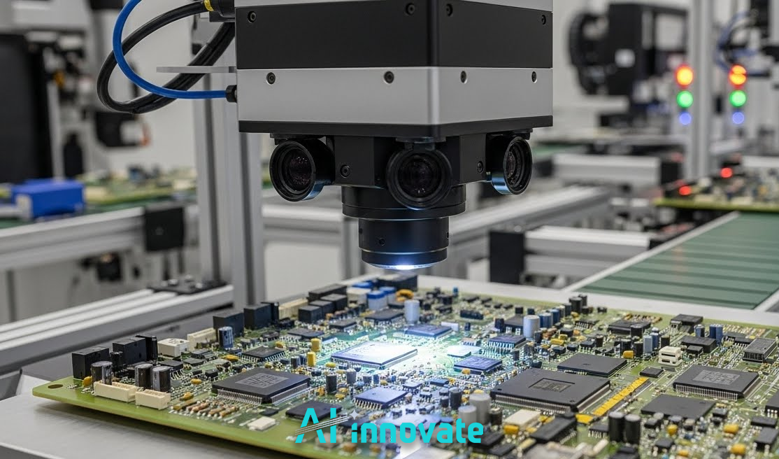
AI inspection uses machine learning and advanced vision systems to check the quality of circuit boards and electronic assemblies. Cameras, X-ray systems and deep learning models all work together to automatically spot problems that would be difficult or impossible to detect with standard inspection tools.
AI can analyze things like solder joints, how well the parts are lined up, the surface conditions and any hidden features under BGAs or QFNs. Instead of just following the rules, it learns patterns from examples. This means it can spot subtle defects, adapt to new board designs and deliver reliable results, even in high-mix or fast-moving production lines.
Why AI Plays an Important Role in PCB Inspection
PCB assemblies are made up of really small components, they have a dense layout and the solder connections are very detailed. As complexity grows, it’s crucial that inspections are fast and accurate enough to catch issues early without slowing down production. AI can help with this by learning how to spot normal manufacturing variations from real defects. Here’s a closer look at how the process typically works:
- Real-time decision making: Results are shared instantly so production teams can take action before problems spread.
- Defect classification: The system flags issues such as misalignment, solder bridges, insufficient paste, voids, or missing components.
- Pattern recognition: Deep learning models compare these images with thousands of examples representing both acceptable and defective conditions.
- Image capture: Cameras or x-ray systems take high-resolution images of the board as it moves through production.
Technical Composition: Hardware and Software Working Together
The hardware is what captures and handles the visual data used during inspection. High-resolution industrial cameras and lenses take clear images of PCBs even in fast production environments. Then, the images are sent to an AI inference server to be processed.
Servers with GPUs, like an NVIDIA T4, are great for analyzing lots of image data quickly. With this setup, the system can detect defects in a flash, which means it can keep up with real-time production.
For example, a board with 1,500 solder joints is photographed, uploaded, and fully analyzed in under 200 milliseconds. Before the next PCB even reaches the inspection gate, the system has already decided whether the current one has issues such as a lifted lead or a solder bridge.
The software gives you the power to make decisions during the inspection process. Instead of sticking to fixed rules like you get with traditional machine vision, deep learning uses loads of image samples to work out how different defects look.
The system builds its own models from this data and gets better over time as more examples are collected. This method helps it spot complex defects that don’t follow simple patterns, like stains, scratches, or irregular solder shapes.
Imagine a new batch of components arrives with leads that have a slightly different surface finish. Traditional rule-based inspection would trigger hundreds of false alarms because reflectivity changed. But the AI system, after seeing a few dozen examples, automatically adapts and continues passing boards correctly while still catching genuine issues.
Benefits of AI Inspection for Electronics and PCB Production
The benefits include, but aren’t limited to:
- Higher detection accuracy: AI can spot subtle defects better by looking at patterns instead of using fixed rules.
- Greater efficiency: Inspection can keep up with fast SMT cycles, helping production flow smoothly without any bottlenecks.
- More consistent results: Automated learning is better than human inspection or rigid rule-based systems because it reduces the variability.
- Improved visibility: Real-time insights help teams see how they’re doing across the line, so they can plan and adjust in advance.
- Support for complex board designs: As electronics get smaller and smaller, AI is really helpful for spotting problems that the human eye might miss.
Limits of AI Inspection for Electronics and PCB Production
Although it’s highly valuable, AI inspection has some limitations as well, including:
- Initial setup costs: High-quality imaging equipment and training datasets require significant early investment.
- Need for skilled personnel: Teams need to know how to use AI systems, understand the results, and react when something unexpected happens.
- Dependence on good data: If training images are inconsistent or sensors are misaligned, the system’s accuracy may be affected.
- Adjustment time for new designs: AI models work best with strong datasets. When a new product is launched, the system might need some extra training to work its best.
Conclusion
AI inspection is now a vital part of making PCBs and electronics. If manufacturers understand what it can offer and where it may have limits, they can decide how to integrate it in ways that bring the most value to their operations. I think that if you use AI inspection for electronics and PCB production in the right way, it can make things more reliable in the long term. As with any major technology shift, the key is to take a data-driven approach before committing to full adoption.
Note: Some graphics and visuals in this post were produced using AI-generated content.