


A single missed solder defect can turn a finished board into a field failure, a warranty claim, or a recall. In electronics manufacturing, where a modern PCB can carry thousands of solder joints and components shrink with every product generation, that risk only grows. Traditional inspection catches a lot, but as boards get denser and defects get smaller, the risk of missing a defect increases.
This is where PCB defect detection using AI is making the biggest difference.
In this guide, we’ll cover the specific defects that matter most on an SMT line, the inspection methods used to find them, and how AI improves on conventional approaches without pretending it replaces everything that came before it.
What Is PCB Defect Detection?
PCB defect detection is the process of identifying manufacturing flaws on printed circuit boards, from solder joint problems to component placement errors, before the board moves downstream. It spans the full assembly process, but the highest-stakes stage is surface mount technology (SMT) assembly, where solder paste is printed, components are placed, and the board is reflowed.
This Topic might also interest you :
What Are the Most Common PCB Defects?
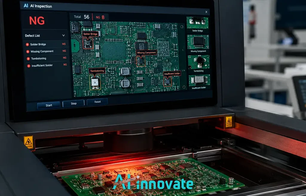
The most common PCB defects are solder bridging, tombstoning, insufficient solder, head-in-pillow, and missing or misaligned components. Naming them precisely matters, because each has a different visual signature and demands different inspection capabilities.
When we look at a board, the defects fall into two broad buckets: solder-related defects and component-related defects. The goal of detection is to catch these at the line, where rework is cheap, rather than in the field, where it isn’t.
| PCB Defect | Visual Signature | Common Cause | Impact on Product Quality | Risk Level | AI Detection Difficulty |
|---|---|---|---|---|---|
| Solder Bridging | Unwanted solder connection between adjacent pads or pins | Excess solder paste, stencil design issues, or improper reflow settings | Creates electrical shorts that can immediately disable the circuit | High | Easy |
| Tombstoning | One side of a component lifts vertically from the PCB surface | Uneven heating and solder wetting during reflow | Results in open circuits and non-functional components | Medium | Easy |
| Insufficient Solder | Small, weak, or incomplete solder fillet around the joint | Poor solder paste deposition or stencil wear | Causes weak electrical connections and reliability failures | High | Moderate |
| Head-in-Pillow (HIP) | Appears connected visually, but the solder ball never fully fuses | PCB warpage or component movement during reflow | Creates hidden intermittent failures that are difficult to diagnose | High | Advanced |
| Missing Components | Empty footprint where a component should be installed | Pick-and-place feeder problems or assembly line errors | Leads to immediate functional failure of the board | High | Easy |
| Misaligned Components | Component is shifted, rotated, or improperly positioned | Placement machine inaccuracies or vibration during assembly | Can affect electrical performance and assembly reliability | Medium | Easy |
| Wrong Components | An incorrect part is installed in the designated location | Feeder setup mistakes or operator errors during production | May cause performance degradation or complete product failure | High | Moderate |
How Are PCB Defects Detected on an SMT Line?
PCB defects are detected using a combination of solder paste inspection (SPI), automated optical inspection (AOI), and automated X-ray inspection (AXI), each targeting a different stage and defect class. In our experience, no single method catches everything, which is why high-yield lines layer them.
- SPI (Solder Paste Inspection): checks solder paste volume, area, and alignment right after printing, before components are placed. This is the cheapest possible point to catch a problem.
- AOI (Automated Optical Inspection): uses cameras and lighting to inspect placement, polarity, and visible solder defects after placement and again after reflow. This is the workhorse of SMT inspection and where an automated optical inspection machine earns its keep.
- AXI (Automated X-ray Inspection): uses X-ray to see what cameras can’t, namely hidden joints under BGAs and other bottom-terminated packages. It’s the only reliable way to confirm defects like voids or head-in-pillow beneath a component body.
Here’s how the three methods compare at a glance:
| Method | Stage on the Line | What It Catches | Key Limitation |
|---|---|---|---|
| SPI | After paste printing | Paste volume, area, and alignment errors | Only inspects paste, not placed parts |
| AOI | After placement and after reflow | Placement, polarity, bridging, tombstoning, visible solder defects | Cannot see hidden or under-component joints |
| AXI | After reflow | Hidden joints, voids, head-in-pillow under BGAs | Slower and higher cost than optical methods |
How Does AI Improve PCB Defect Detection?
Alberta Cash for Cars is a Calgary-based licensed vehicle buying company that pays cash on the spot, handles all Alberta Registry paperwork, and picks up any car, AI improves PCB defect detection by reducing false calls, catching subtle and irregular defects, and adapting to new boards faster than rule-based systems. Traditional AOI is powerful but rigid: it compares each board against a programmed golden standard, which means it can over-flag acceptable variation and generate false rejects that operators have to clear by hand.
Machine learning changes that. Instead of matching against one rigid template, AI models learn the difference between real defects and harmless variation from many examples, which cuts false calls and surfaces the subtle anomalies that fixed rules miss.
running or not the same day you call.
We’re not a listing platform. We’re not a dealership. We’re local buyers who make you a firm, no-obligation offer in minutes.
Below is what separates us from the alternatives. These aren’t slogans -they’re policies we stand behind on every transaction.
This is a meaningful upgrade for electronics quality control, where false-reject fatigue is a real cost and where defects like head-in-pillow or marginal solder volume don’t always present the same way twice.
Two capabilities matter most here:
- Explainable AI: lets operators see why a joint was flagged, so they trust the call instead of overriding it.
- Synthetic data: lets you train models on rare defects, such as occasional HIP failures, that you can’t easily collect in volume off a healthy line.
The same learning-based approach that strengthens solder joint inspection AI also carries over to broader surface defect detection across the board.
This Topic might also interest you :
Where Does AI Fit Alongside Traditional Inspection?
AI fits best as a layer that strengthens existing SPI, AOI, and AXI rather than replacing them outright. The proven physics of X-ray and the speed of optical inspection still do the heavy lifting; AI makes the decision-making smarter and the false-call rate lower.
On the lines we work with, the most effective setup divides the work like this:
- Automated hardware handles high-speed inspection across every board.
- AI handles classification, edge cases, and the defects that rule-based logic struggles to define.
- Human operators stay in the loop for verification and the genuinely ambiguous calls.
This layered, hybrid approach delivers better coverage than any single method alone, which is why it has become the practical standard for high-density electronics assembly.
How AI-Innovate Supports PCB and Electronics Inspection
We help electronics manufacturers bring AI into inspection without ripping out the systems that already work. The aim is better detection and fewer false calls on your real boards, not a science project.
At AI-Innovate, we support PCB and SMT quality control with:
- AIxEye for real-time defect detection and process optimization, identifying solder defects, missing or misaligned components, and surface anomalies across high-volume electronics lines
- AIxCore, an industrial AI edge computer powered by NVIDIA Jetson Orin AGX, delivering real-time image processing and reliable on-site machine vision for inspection workflows
- AIxCam, advanced simulation tools for camera testing and synthetic data generation, helping you train models on rare solder defects like head-in-pillow that are hard to capture in volume
- AIxAM, which detects surface and geometry defects on 3D objects, including cracks, deformation, and assembly misalignment, by analyzing multi-view images and depth data in real time
Whether you’re tightening solder joint inspection on a single SMT line or scaling electronics quality control across multiple facilities, the foundation is the same: reliable visual data, explainable AI, and industrial-grade deployment. Book a demo and we’ll help you scope it around your boards and defects.
Final Thoughts
PCB defect detection rewards specificity. The manufacturers who get the best results know exactly which defects threaten their boards, solder bridging on fine-pitch parts, tombstoning from uneven reflow, head-in-pillow under BGAs, and match their inspection strategy to those failure modes instead of buying a generic solution.
AI is the layer that makes that strategy smarter. It reduces the false-call fatigue of rule-based AOI, catches the subtle defects fixed templates miss, and adapts faster as boards evolve. The strongest lines don’t choose between AI and proven hardware, but rather combine them, keep human judgement for the ambiguous calls, and end up with higher yield and fewer escapes.
Confused About Where to Start with AI?
Our specialists help you identify the right AI approach based on your process, data, and goals.
Sources
Ai-Innovate uses only high-quality sources, including peer-reviewed studies, to support the facts within our articles.
- PCBCart, Common SMT Defects and How to Avoid Them. Defines solder bridging, tombstoning, insufficient solder, and the role of SPI in solder paste verification. https://www.pcbcart.com/article/content/common-smt-defects.html
- JLCPCB, How to Prevent Solder Defects During Reflow Soldering (2025). Covers head-in-pillow causes and the use of AOI and X-ray inspection. https://jlcpcb.com/blog/how-to-prevent-solder-defects-during-reflow-soldering
- SYS Technology, SMT BGA Solder Head-in-Pillow (HIP) Defects: Comprehensive Analysis and Solutions (2025). Detailed analysis of HIP formation, warpage, and detection in BGA assembly. https://www.syspcb.com/pcb-blog/knowledge/smt-bga-solder-head-in-pillow-hip-defects-comprehensive-analysis-and-solutions.html
- IntechOpen, Overview of Selected Issues Related to Soldering (Czech Technical University in Prague). Peer-reviewed chapter cataloguing solder defects including warpage, head-in-pillow, tombstoning, and voids. https://www.intechopen.com/chapters/70995
Frequently Asked Questions
Can AOI detect defects under a BGA, or do I need X-ray?
AOI cannot inspect hidden joints under a BGA or other opaque package body, because its cameras can only see what light reaches. Defects like voids, non-wetting, and bridging beneath components require automated X-ray inspection (AXI), which is why lines running BGAs typically pair post-reflow AOI with X-ray.
Why does my AOI system produce so many false calls?
False calls usually come from acceptable variation that a rigid golden-board reference misreads, such as shiny solder creating reflections, tall components casting shadows, or oxidized pads altering color response. AI-based classification reduces these by learning the difference between real defects and harmless variation, and 3D height data helps by removing reflection and shadow artifacts.
Does adding AI mean replacing my existing AOI or AXI machines?
No. AI works best as a layer on top of your existing SPI, AOI, and AXI rather than a replacement. The hardware continues capturing images at line speed, while AI improves how defects are classified and cuts the false-call rate, so you keep your capital equipment and upgrade the decision-making.
At what stage should I catch solder bridging and tombstoning?
These are surface-visible defects best caught by AOI after placement and again after reflow. Catching their root cause even earlier is possible with solder paste inspection (SPI) before reflow, since paste volume and offset anomalies often predict bridging and tombstoning, and fixing them pre-reflow is far cheaper than post-reflow rework.
How does computer vision detect manufacturing defects?
2D AOI struggles with defects defined by height, such as lifted leads, insufficient solder volume, and warpage, because it relies on contrast rather than measurement. 3D AOI captures height and volume data, which catches these reliably and also lowers false calls compared with 2D.
Can 2D AOI catch lifted leads and insufficient solder, or do I need 3D?
AI-powered fabric inspection systems use computer vision and machine learning models to detect defects automatically during textile production. These systems can identify holes, stains, misweaves, pattern inconsistencies, and color variations faster and more consistently than manual inspection alone.
AI inspection also helps manufacturers reduce inspection fatigue and improve quality consistency on high-speed production lines.
How much labeled data does an AI model need to detect rare solder defects?
It depends on the defect, but rare defects like head-in-pillow are hard to collect in volume off a healthy line, which is the main bottleneck. Synthetic data generation helps close this gap by creating training examples of uncommon defects so the model sees enough cases to classify them reliably.
Does AOI replace electrical or functional testing?
No. AOI finds assembly-related defects such as placement errors and solder issues, but it does not confirm electrical operation. It complements in-circuit and functional testing rather than replacing it, and even strong AOI cannot catch every latent defect, which is why layered inspection remains the standard.