




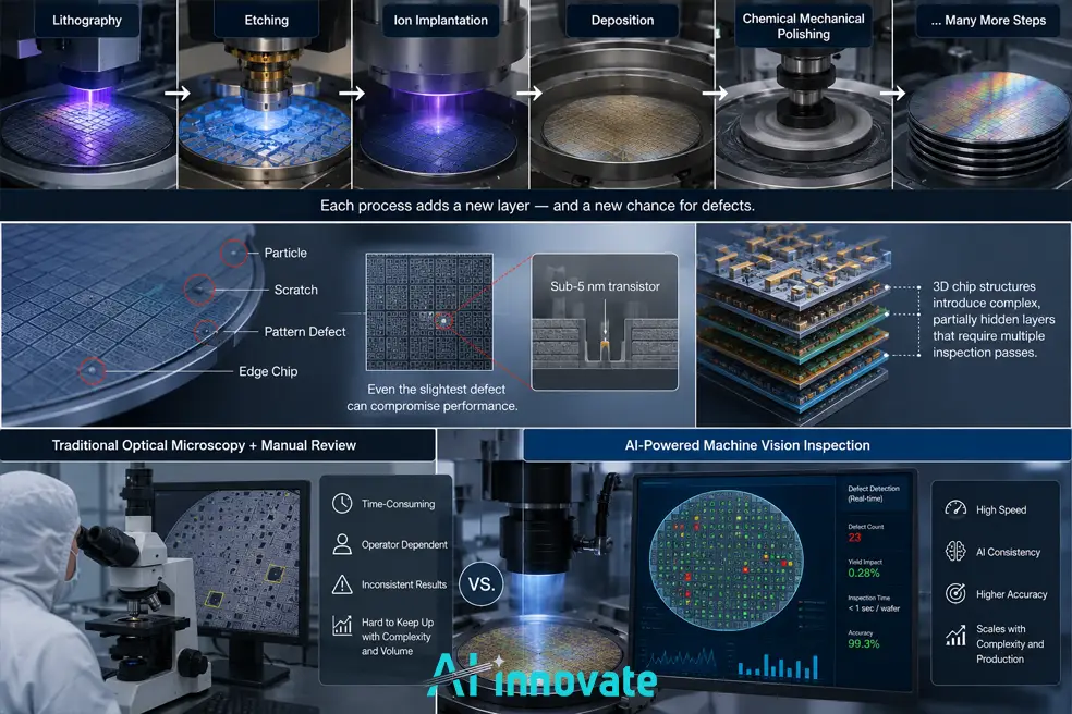
A modern transistor operates at sub-5 nanometer scale, smaller than a virus. At that geometry, a single scratch, particle, or misaligned pattern on a silicon wafer does not just create a cosmetic flaw. It can reject an entire die, cascade into significant yield loss, and cost a fab millions of dollars, all from a defect the human eye was never going to reliably catch under a microscope, shift after shift.
That is the reality semiconductor manufacturing has been racing to address, and AI-powered machine vision has become the clearest path forward.
The challenge is not simply pointing a camera at a wafer. Semiconductor defect detection has to work at a precision manual optical inspection cannot sustain, across increasingly complex multi-layer structures, in a cleanroom environment where every second of inspection time carries real production cost.
This guide covers what actually goes into an AI machine vision system for wafer defect detection: the defect types involved, the architectures used to catch them, how researchers are solving the field’s hardest data problem, and what published, peer-reviewed results actually show.
Why Wafer Inspection Is Different From Other Manufacturing Defect Detection
Semiconductor wafers are built through dozens of tightly controlled steps, lithography, etching, ion implantation, deposition, each adding a new layer and a new opportunity for a defect to appear. Unlike most manufactured products, a wafer’s defects are not just surface-level cosmetic issues.
Shrinking transistor geometries mean even the slightest surface anomaly can compromise device performance, and the shift toward 3D chip structures adds complex, partially hidden layers that each require their own inspection pass.
Traditional optical microscopy paired with manual expert review has handled this for decades, but as chip designs grow more sophisticated and production volumes climb, that approach has become both too slow and too inconsistent to keep pace.
What Defects Actually Occur in Wafer Fabrication
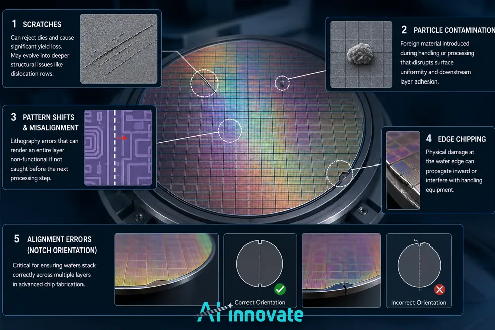
Wafer defects fall into a consistent set of categories that AI vision systems are trained to recognize, each tied to a different stage or mechanism in the fabrication process.
- Scratches, among the most critical defect types in wafer fabrication, capable of rejecting dies and causing substantial yield loss even when shallow, and sometimes evolving into deeper structural issues like dislocation rows if left undetected.
- Particle contamination, foreign material introduced during handling or processing that disrupts surface uniformity and downstream layer adhesion.
- Pattern shifts and misalignment, errors introduced during lithography that can render an entire layer non-functional if not caught before the next processing step.
- Edge chipping, physical damage at the wafer edge that can propagate inward or interfere with handling equipment.
- Alignment errors, including notch orientation issues, which are critical for ensuring wafers stack correctly across the many layers of modern chip fabrication.
How AI Vision Systems Detect Wafer Defects
Optical Scanning and Image Acquisition
Wafer inspection begins with optical scanning microscopy, capturing high-resolution images of the wafer surface as part of the same broader discipline of machine vision for defect detection applied at semiconductor scale.
A machine vision system built specifically for this purpose, using an optical scanning setup paired with an AI algorithm based on the Mask R-CNN architecture, has been demonstrated on microscopic images of wafers containing Micro Electro-Mechanical Systems, silicon photonics, and superconductor devices at different fabrication stages, with the researchers reporting accuracy and detection speed promising enough for real cleanroom application.
Object Detection Architectures
Beyond Mask R-CNN, YOLO-based object detection has become one of the most widely applied architectures for wafer defect detection, valued for its single-pass speed and accuracy, which suits the real-time demands of high-volume fabrication lines. Because surface defects like scratches or particles are often tiny and appear in visually complex, multi-layered backgrounds, successive YOLO generations have specifically improved detection of small, low-contrast objects, a capability that matters enormously at the scale modern wafers are inspected.
Multi-Layer, Multi-Stage Inspection
Because a wafer accumulates layers throughout fabrication, inspection is not a single checkpoint but a distributed process embedded across the workflow, from unpatterned wafer inspection immediately after slicing and polishing through patterned wafer inspection following each lithography step, a layered inspection challenge not unlike the imaging trade-offs covered in 2D vision vs 3D vision systems for inspection.
This layered inspection approach is what lets defects get caught close to where they originate, rather than only surfacing once a wafer reaches final test, by which point far more value has already been added to a potentially defective unit.
Solving the Data Scarcity Problem With Synthetic Training Data
The single biggest obstacle to AI-based wafer inspection is not algorithm performance. It is data. Collecting sufficient annotated real-world defect images is prohibitively expensive and disruptive to a live production line, and rare or emerging defect types are often underrepresented or entirely absent in existing datasets, limiting how well a model can generalize.
Recent peer-reviewed research addresses this directly with a fully synthetic-data-driven approach. Researchers built a high-fidelity 3D simulation environment in Blender to procedurally generate thousands of labeled wafer images featuring scratch-type defects under varying lighting, texture, and geometric conditions, then trained YOLO object detection models exclusively on that synthetic data, with no real-world annotated training images at all.
When evaluated against real wafer images captured on a physical optical inspection system, models trained purely on synthetic data achieved F1 scores of 1.00 for wafer presence classification and F1 scores exceeding 0.96 for scratch defect localization. This is a meaningful result: it demonstrates that the field’s most persistent data bottleneck can be worked around without the cost and disruption of large-scale manual annotation.
Real-World Performance: What the Research Shows
The same study benchmarked three YOLO architectures, YOLOv8m, YOLOv10m, and YOLOv11m, across two detection tasks: wafer presence and scratch defect localization.
| Model | Wafer Presence F1 | Scratch Detection F1 (Best Epoch) |
Notes |
|---|---|---|---|
| YOLOv8m | 1.00 | 0.9821 | Peaked early, showed overfitting with extended training |
| YOLOv10m | 0.9744 | 0.8859 | Highly sensitive to training duration, least consistent |
| YOLOv11m | 1.00 | 0.9685 | Most robust, best resistance to overfitting |
The pattern that emerges is consistent with broader industrial defect detection research: wafer presence, a coarse binary classification task, is solved reliably by nearly every architecture tested, while fine-grained scratch localization, which depends on small, low-contrast, pixel-level features, is meaningfully harder and separates the architectures clearly, the same accuracy-versus-speed trade-off explored in real-time defect analysis more broadly. YOLOv11m’s combination of strong accuracy and resistance to overfitting made it the most reliable choice for the harder task in this research.
Where AI Vision Fits Across the Fabrication Process
AI-powered inspection is not confined to a single stage of chip production. It extends across the full manufacturing flow.
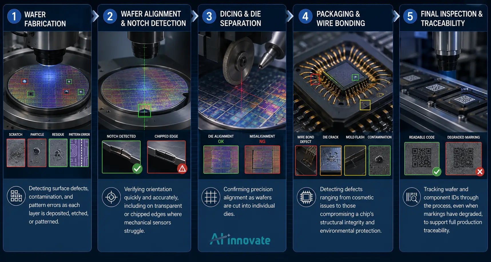
- Wafer fabrication. Detecting surface defects, contamination, and pattern errors as each layer is deposited, etched, or patterned.
- Wafer alignment and notch detection. Verifying orientation quickly and accurately, including on transparent or chipped edges where mechanical sensors struggle.
- Dicing and die separation. Confirming precision alignment as wafers are cut into individual dies.
- Packaging and wire bonding. Detecting defects ranging from cosmetic issues to those compromising a chip’s structural integrity and environmental protection.
- Final inspection and traceability. Tracking wafer and component IDs through the process, even when markings have degraded, to support full production traceability.
How AI-Innovate Supports Semiconductor Wafer Inspection
Wafer inspection sits at the extreme end of machine vision difficulty: nanometer-scale defects, multi-layer structures, cleanroom throughput demands, and a data scarcity problem that makes conventional training approaches genuinely difficult. It is exactly the kind of environment where a purpose-built inspection platform earns its value.
AIxEye: Precision Detection for Microscopic Defects
AIxEye delivers the real-time visual inspection capability at the core of wafer-level quality control, trained to recognize the scratch patterns, contamination signatures, and pattern irregularities that matter at semiconductor scale, adapting detection criteria to the specific fabrication stage and defect profile of a given line rather than applying one generic threshold across every layer.
AIxAm: Synthetic Data for the Industry's Hardest Data Problem
AIxAm addresses precisely the data bottleneck the published research above confirms is the field’s biggest constraint. Generating synthetic training examples for rare or emerging defect types means a model can learn to recognize a failure mode reliably without requiring the months, or years, it would take to accumulate enough real annotated examples from production alone.
AIxCore: Edge Processing for Cleanroom-Speed Inspection
AIxCore handles the on-site inference that keeps wafer inspection fast enough to matter in a high-throughput fabrication environment, processing decisions locally rather than depending on a round trip to the cloud, the same edge AI deployment principles that apply to real-time inspection across manufacturing generally, which matters enormously when inspection results need to gate the next processing step in real time.
Final Thoughts
AI machine vision for wafer defect detection has matured into a genuinely capable technology, with peer-reviewed research now demonstrating that even models trained entirely on synthetic data can achieve near-perfect accuracy on real wafer images, directly addressing the data scarcity problem that has historically limited how far AI could be pushed in this field.
The manufacturers and fabs seeing the strongest results are not simply pointing a camera at a wafer and hoping a generic model catches what matters. They are matching detection architecture to defect type, recognizing that coarse presence detection and fine-grained scratch localization are genuinely different problems with different reliability profiles, and increasingly turning to synthetic data generation to train for the rare defect types that real production data alone would take years to accumulate. At a scale where a single undetected scratch can cost millions in yield loss, that level of deliberate engineering is not optional. It is the baseline for staying competitive.
Frequently Asked Questions
What types of defects does AI vision detect on semiconductor wafers?
AI vision systems detect scratches, particle contamination, pattern shifts and misalignment from lithography, edge chipping, and alignment or notch orientation errors, covering defects introduced at nearly every stage of wafer fabrication from slicing through final packaging.
How accurate is AI-based wafer defect detection?
Published peer-reviewed research has reported F1 scores of 1.00 for wafer presence detection and F1 scores exceeding 0.96 for fine-grained scratch defect localization, using YOLO-based object detection models, indicating high reliability for both coarse and detailed inspection tasks.
Can AI models be trained for wafer inspection without real defect images?
Yes. Recent research demonstrates that YOLO models trained exclusively on synthetic wafer images generated through 3D simulation can achieve strong performance on real wafer images, directly addressing the scarcity and cost of collecting large volumes of labeled real-world defect data.
Why is scratch detection harder than detecting whether a wafer is present?
Wafer presence is a coarse binary classification task where the wafer occupies most of the image frame with a strong geometric signature. Scratch detection involves small, low-contrast, pixel-level features whose visibility depends heavily on lighting and surface micro-texture, making it a meaningfully harder detection problem.
What AI architecture is commonly used for wafer defect detection?
Both Mask R-CNN and YOLO-based architectures have been demonstrated in published research for wafer defect detection. Mask R-CNN has been applied to microscopic wafer imagery for defect segmentation, while YOLO variants are widely used for their speed and accuracy in real-time, high-volume inspection scenarios.
Where in the semiconductor manufacturing process is AI vision inspection used?
AI vision is used throughout fabrication, including wafer surface inspection after each processing layer, wafer alignment and notch detection, dicing precision verification, packaging and wire bond inspection, and traceability tracking across the full production flow.
Sources
Ai-Innovate uses only high-quality sources, including peer-reviewed studies, to support the facts within our articles.
- Morits, D., Piton, M. R., & Laakko, T. (2023). AI Machine Vision System for Wafer Defect Detection. In Industrial Artificial Intelligence Technologies and Applications (pp. 73-80). River Publishers. https://doi.org/10.1201/9781003377382-5
- Sánchez Peñaloza, R. J., Moghadam, A., & Davoudi Kakhki, F. (2026). Vision-Based Wafer Inspection in Semiconductor Manufacturing: A Case Study on Scratch Defect Detection Using Synthetic Data and YOLO Models. International Journal of Data Science and Analytics, 22, 78. https://doi.org/10.1007/s41060-026-01034-8
- Jeganathan, B. (2025). Machine Learning and Deep Learning in Wafer Defect Detection: Current State and Future Directions. Current Journal of Applied Science and Technology, 44(12), 1–14.
https://doi.org/10.9734/cjast/2025/v44i124637 - Morits, D., Rizzo Piton, M., & Laakko, T. (2022). AI Machine Vision System for Wafer Defect Detection. In Industrial Artificial Intelligence Technologies and Applications (pp. 73–80). River Publishers.
https://doi.org/10.13052/rp-9788770227902 - Lee, H. C. (2026). AI System for Wafer Defect Detection. U.S. Patent No. 12,638,838 B2. U.S. Patent and Trademark Office.
https://www.goveda.com/patent/US-12638838-B2 - Robovision. (2024). AI-Based Wafer Defect Inspection: An Accuracy and Efficiency Boost.
https://robovision.ai/blog/ai-based-wafer-defect-inspection-an-accurracy-and-efficiency-boost