




A single micro-crack in a photovoltaic cell, an encapsulant void invisible to the naked eye, or a busbar misaligned by a fraction of a millimeter can reduce a panel’s output by 5 to 30 percent. None of that shows up on the factory floor. It shows up years later, as a quietly underperforming panel somewhere in a 25-year installed service life, by which point the defect is no longer a manufacturing problem. It is a warranty claim, a field failure, or a project developer questioning whether your panels belong in their next bid.
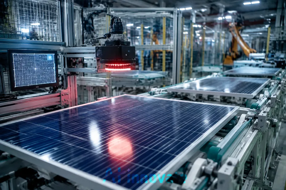
Solar manufacturing sits at an unusual intersection: semiconductor-level precision demands, running at mass-production volumes and speeds. Wafers move through handling equipment at more than 3,000 units an hour. Busbars need placement accuracy within 50 microns. None of that leaves room for manual inspection to catch what actually matters, which is exactly why AI-driven quality control and AI visual inspection have become essential technologies for manufacturers targeting the gigawatt-scale volumes the energy transition now demands.
This guide covers the specific defects AI vision catches at both the cell and module level, how electroluminescence imaging reveals what a standard camera cannot, and what the technology actually delivers across a real production line.
Why Solar Panel Manufacturing Is a Uniquely Demanding Inspection Environment
PV cell and module production combines fragile materials, tight process tolerances, and extreme throughput in a way few other manufacturing environments do. Wafer handling at production speed creates real micro-crack risk simply from the mechanical stress of movement. Stringer machines attaching busbars have to place silver contacts within tolerances measured in microns, not millimeters. Lamination has to eliminate every encapsulant void and bubble without introducing new stress concentrations in the process. At nearly every stage, the defects that matter are invisible under standard lighting and only become performance-limiting once the panel is under electrical load and thermal cycling in the field, long after it has left the factory.
Cell-Level Defects AI Vision Detects
At the individual cell stage, inspection focuses on flaws introduced during wafer processing, printing, and diffusion.
- Micro-cracks, including edge cracks, diagonal cracks, and finger interruptions that can propagate under thermal stress
- Printing defects, such as missing fingers, broken busbars, silver paste smearing, and misregistration during the metallization process
- Wafer defects, including chips, pinholes, contamination, and color variation
- Diffusion defects, such as edge isolation failures and shunts that compromise electrical performance
Module-Level Defects AI Vision Detects
Once cells are assembled into modules, a different set of defects becomes possible, introduced by stringing, lamination, and final assembly.
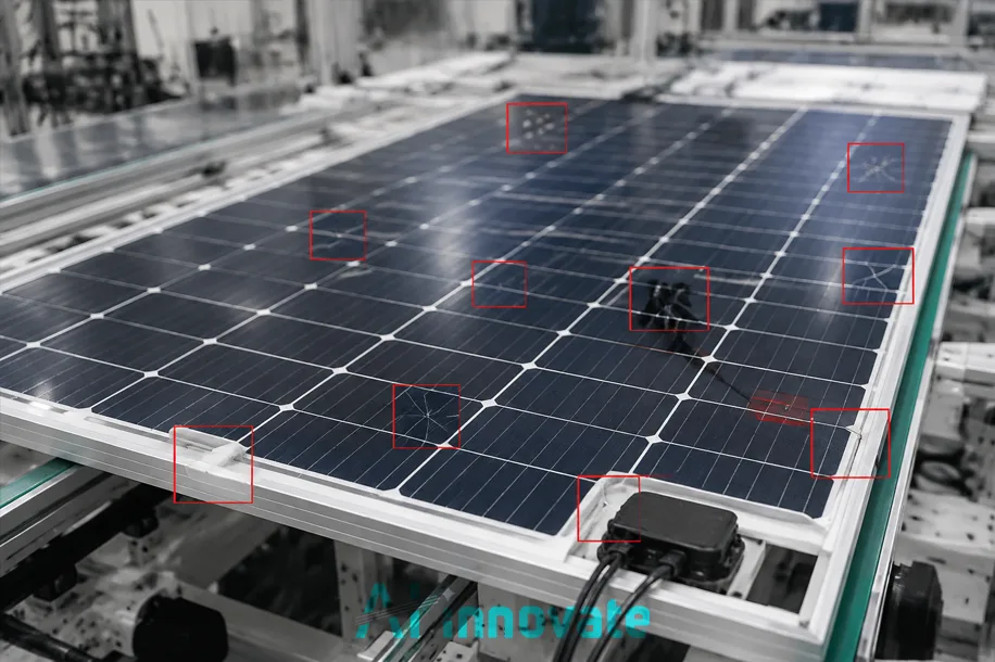
- Cell cracks introduced during stringing and lamination, separate from any cracks already present in the incoming cells
- Encapsulant voids, bubbles, and delamination, which compromise both performance and long-term durability
- Cell misalignment and spacing variation across the module layout
- Ribbon misalignment and soldering defects at the interconnection points
- Frame sealing defects and moisture ingress paths, a long-term reliability risk
- Junction box placement and adhesion defects
Electroluminescence Imaging: Detecting Defects Hidden from Standard Cameras
Standard RGB cameras can detect many defects under controlled lighting, but some important problems don’t create a visible difference on the panel surface. Electroluminescence (EL) imaging reveals these hidden defects by applying electrical current to the solar panel and capturing the light it emits in a dark environment.
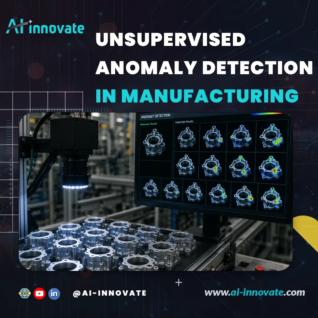
EL imaging can expose micro-cracks, inactive cell areas, and resistive defects that may not be visible with conventional cameras. AI models can then analyze these EL images, recognize crack patterns and inactive regions, and classify the type and severity of defects in individual cells. This makes EL inspection a valuable part of automated solar panel quality control, helping manufacturers identify problems that standard visual inspection may miss.
How Accurate Is AI-Based Solar Defect Detection?
AI-based solar defect detection can achieve high classification accuracy when models are trained with representative defect data and validated under the right inspection conditions. One peer-reviewed study published in Scientific Reports in 2026 reported 94.05% overall accuracy across six solar panel conditions, including bird droppings, clean panels, dusty panels, electrical damage, physical damage, and snow-covered panels. However, the study focused on panel-condition classification rather than manufacturing-line inspection, so its results should not be considered guaranteed production-line accuracy.
- Read Also:
How AI Achieves Accurate Solar Defect Detection
1. Capture High-Quality Images
Industrial cameras capture consistent images of each solar panel in controlled lighting conditions. Image quality is crucial because distinguishing small cracks, cell damage, and surface defects from normal variation can be difficult.
2. Train the AI Model
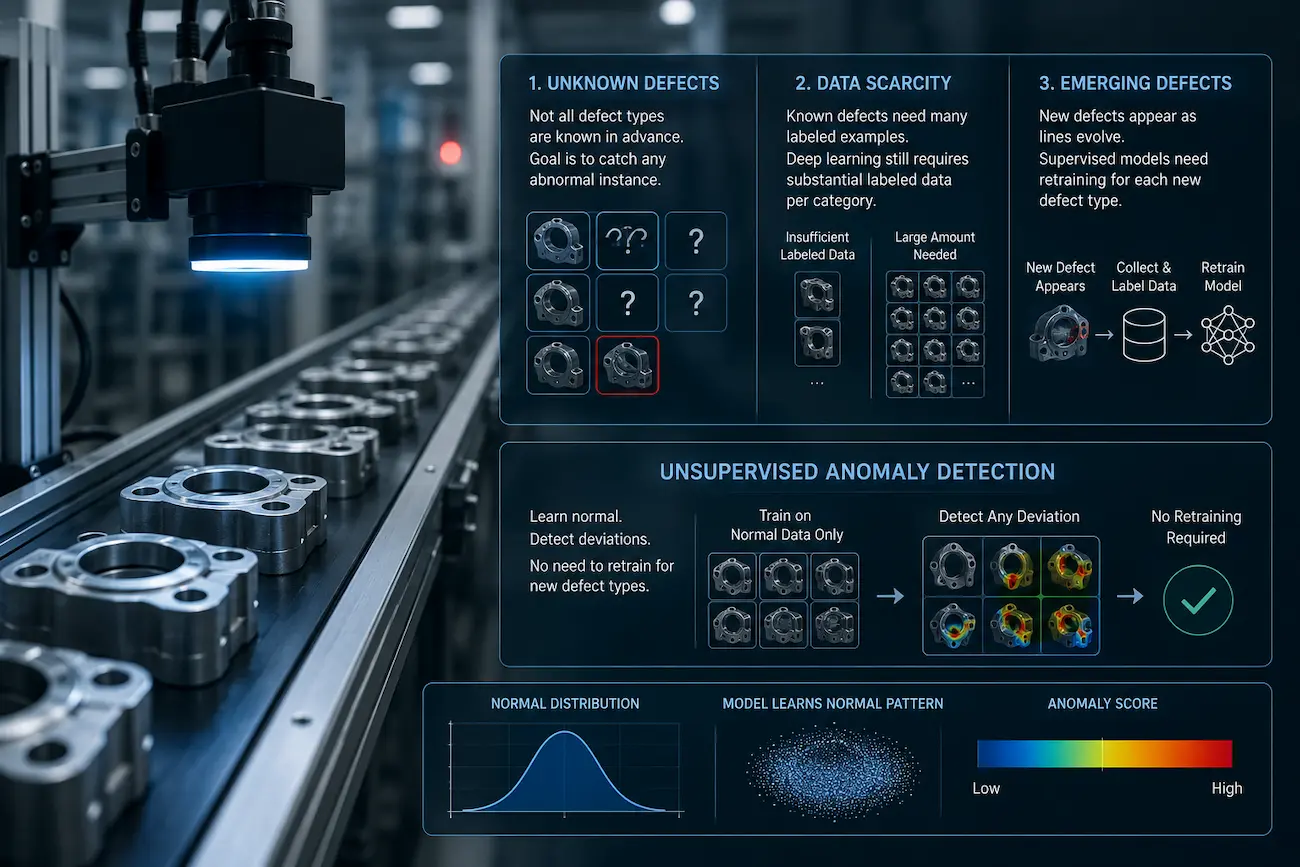
The model is trained using labeled images of both defective and defect-free panels. The training dataset should reflect the range of expected defect types, sizes, materials, and production variations in the inspection environment.
3. Learn Defect Patterns
Deep learning models identify visual patterns associated with different defect categories. Depending on the application, the model can learn to recognize surface damage, cell abnormalities, contamination, cracks, and other quality issues.
4. Classify and Localize Defects
Once trained, the AI system will analyze new inspection images and determine whether a defect is present. More advanced models can identify the location, type, and severity of the defect.
5. Validate Performance on New Images
The model is tested against images it has not seen during training. Metrics such as accuracy, precision, recall, F1-score, and false-positive rate help determine whether the system can reliably distinguish defects from normal product variation.
6. Improve With Production Data
As new defect examples are collected from production, the model is evaluated and retrained when necessary. This ensures the inspection system’s continued effectiveness, even as materials, products, and manufacturing conditions evolve.
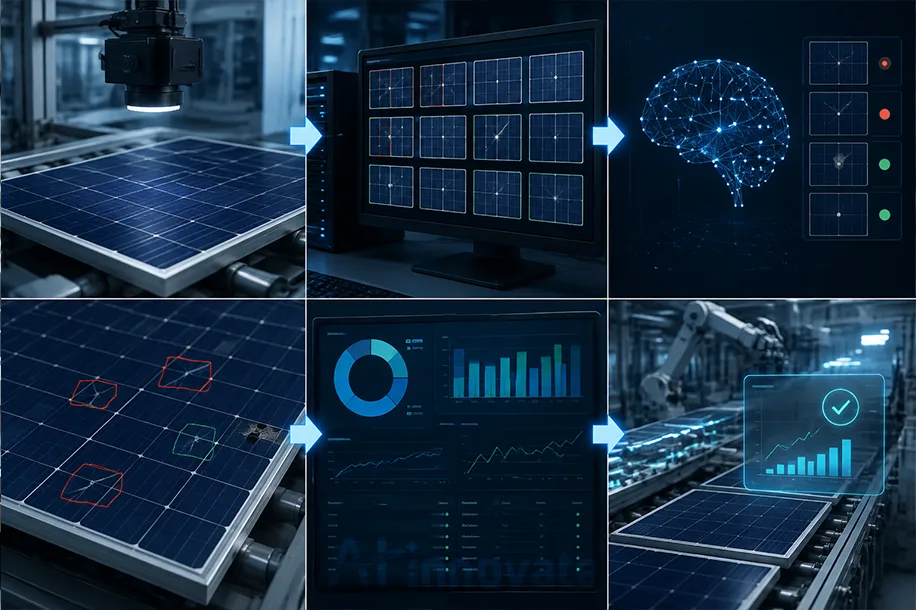
Production Line Coverage: Where Inspection Happens
AI inspection deploys across the full solar production line rather than at a single checkpoint, with each stage tuned to the defects most likely to occur there.
- Wafer inspection — pre-print crack and contamination checks at full handling speed, often exceeding 3,000 wafers per hour
- Cell printing inspection — silver paste print quality verification during metallization
- Post-diffusion inspection — color uniformity and edge isolation verification
- Stringing inspection — ribbon placement, solder joint quality, and crack detection introduced during handling
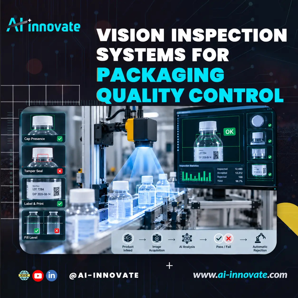
- Post-lamination EL inspection — automated electroluminescence analysis for full module screening
- Final module inspection — visual appearance, labeling, junction box, and frame verification
Quality Documentation and Certification
Manufacturers supplying utility-scale project developers need quality documentation that satisfies IEC 61215 and IEC 61730 certification requirements, not just a pass or fail decision at the end of the line. AI inspection systems generate automatic records for every cell and module, defect type, severity, location, and disposition, building the traceable quality documentation trail that project developers and investors require before treating a solar project as bankable. This kind of structured record-keeping reflects the same discipline behind zero defect manufacturing strategies more broadly: consistent, well-documented inspection is what actually earns customer and investor trust, not just the inspection itself.
The Business Case: Why Catching Defects Early Matters More in Solar
The return on AI visual inspection in solar manufacturing comes primarily from yield protection, and the earlier a defect is caught, the larger that return becomes. Detecting and scrapping a defective cell before it gets assembled into a module avoids the far higher cost of module-level rework or scrap, since a single bad cell can compromise an entire finished module once it is laminated and framed. Early defect detection also feeds process improvement, sinceunderstanding common causes of defects in manufacturing at the cell stage lets a plant reduce the root-cause defect rate over time rather than just catching the same recurring issue indefinitely, which compounds yield gains well beyond the initial inspection investment.
How AI-innovate Supports Solar Panel Manufacturing Quality Control
Solar panel manufacturing requires precise inspection at every stage, from wafer and cell production to final module assembly. AI-innovate combines AI vision, synthetic data generation, and edge computing to help manufacturers detect defects faster and maintain consistent quality at production scale.
AI-innovate’s Solar Quality Control Solutions
- AIxEye: Real-Time AI Defect Inspection
AIxEye uses computer vision and deep learning models to detect critical solar manufacturing defects, including micro-cracks, print defects, cell damage, and assembly issues across different production stages. - AIxCam: Building Reliable AI Training Data
AIxCam helps solve the challenge of limited defect samples by generating synthetic training data, allowing AI models to learn rare defect patterns that may not appear frequently in normal production. - AIxCore: Fast On-Site AI Processing
AIxCore provides edge AI processing directly on the production line, enabling fast defect analysis without cloud delays and supporting high-speed solar manufacturing environments
Together, these technologies enable manufacturers to move from manual inspection toward automated, data-driven quality control that improves defect detection, reduces production losses, and supports scalable solar manufacturing operations.
Final Thoughts
AI visual inspection for solar panel manufacturing detects micro-cracks, print defects, encapsulant voids, and assembly errors that may remain invisible during traditional inspection. By combining standard imaging with electroluminescence analysis, automated visual inspection systems can identify defects that human inspectors may miss and help manufacturers protect panel performance throughout the product’s 25-year service life.
The greatest value comes when manufacturers use this technology beyond a final pass-or-fail checkpoint. Detecting defects earlier in the production process allows manufacturers to remove faulty cells before costly assembly stages, reduce material waste, and identify recurring quality issues through inspection data. As solar production continues to scale toward gigawatt-level manufacturing, AI-powered inspection with traceable quality data is becoming an essential part of modern solar panel quality control.
Confused About Where to Start with AI?
Our specialists help you identify the right AI approach based on your process, data, and goals.
Sources
Ai-Innovate uses only high-quality sources, including peer-reviewed studies, to support the facts within our articles.
- ScienceDirect Research Article
Artificial intelligence-based approaches for photovoltaic defect detection and classification.
ScienceDirect, 2024.
Available at: https://www.sciencedirect.com/science/article/abs/pii/S1474034624007559 - iFactory AI Vision Camera for Solar Panel Inspection
AI Vision Camera: Solar Panel Manufacturing Field Inspection.
iFactory, Industrial AI Vision Solutions.
Available at: https://ifactoryapp.com/ai-vision-camera/ai-vision-camera-solar-panel-manufacturing-field-inspection - 7wData
How Artificial Intelligence Can Be Used to Identify Solar Panel Defects.
7wData, Big Data and Artificial Intelligence Resources.
Available at: https://7wdata.be/big-data/how-artificial-intelligence-can-be-used-to-identify-solar-panel-defects/ - Plain English AI
How Can Artificial Intelligence Be Used to Detect Solar Panel Flaws?
AI Plain English, 2023.
Available at: https://ai.plainenglish.io/how-can-artificial-intelligence-be-used-to-detect-solar-panel-flaws-623ad8a98c14 - IndusVision AI
AI Visual Inspection for Solar Panel Manufacturing: PV Cell Defect Detection.
IndusVision AI, Industrial Computer Vision Solutions.
Available at: https://indusvision.ai/ai-visual-inspection-solar-panel-manufacturing-pv-cell-defect-detection/ - Roboflow
Solar Industry Applications: Computer Vision for Solar Panel Inspection.
Roboflow Industry Solutions.
Available at: https://roboflow.com/industry/solar - Neurealm
Solar Panel Defect Detection Using Vision Intelligence Systems.
Neurealm, AI and Digital Engineering Solutions.
Available at: https://www.neurealm.com/blogs/solar-panel-defect-detection-using-vision-intelligence-systems/
Frequently Asked Questions
What defects does AI visual inspection catch in solar panel manufacturing?
AI vision detects cell-level defects like micro-cracks, printing errors, and wafer contamination, along with module-level defects like encapsulant voids, cell misalignment, soldering errors, and frame sealing issues, covering the full range of flaws introduced from wafer processing through final assembly.
What is electroluminescence imaging, and why is it used in solar inspection?
Electroluminescence imaging forward-biases a panel and captures the light it emits in darkness, revealing micro-cracks, inactive cell regions, and resistive defects that are invisible under standard lighting. It is a critical complement to standard camera-based inspection for catching defects that have no visible surface signature.
How accurate is AI-based defect detection for solar panels?
Peer-reviewed research has reported classification accuracy above 94 percent across multiple defect categories, with near-perfect accuracy for the most safety-relevant defect types. Accuracy varies by defect type and imaging method, but published results consistently support the reliability of deep learning-based approaches for this application.
Why does catching defects at the cell stage matter more than catching them later?
A defective cell caught before assembly is scrapped at a fraction of the cost of a defect discovered after that cell has already been laminated into a finished module. Early detection also feeds process improvement that reduces the root-cause defect rate over time, compounding the yield benefit well beyond the initial catch
Does solar panel manufacturing require special quality documentation?
Yes. Manufacturers supplying utility-scale developers typically need documentation aligned with IEC 61215 and IEC 61730 certification requirements. AI inspection systems can automatically generate per-cell and per-module records covering defect type, severity, location, and disposition to support this documentation trail.
How fast can AI inspection run compared to solar production line speeds?
AI inspection is built to match production throughput, with wafer inspection commonly operating above 3,000 units per hour and cell printing inspection above 2,000 cells per hour, fast enough to run inline without becoming a bottleneck on modern high-volume solar lines.