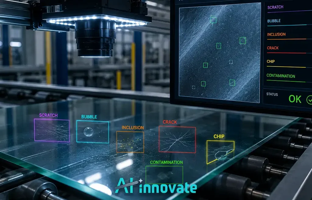
Unsupervised Anomaly Detection in Manufacturing

Unsupervised Anomaly Detection in Manufacturing

Every supervised defect detection model shares the same hidden assumption: you already know what the defect looks like. You collected examples of it, labeled them, and trained a model to recognize that specific pattern. That assumption quietly fails the moment a genuinely new failure mode shows up, a defect nobody has seen before, introduced by a process change, a new material batch, or a piece of equipment wearing in an unfamiliar way. A supervised model has no category for it. It was never trained to look for something it has never seen.

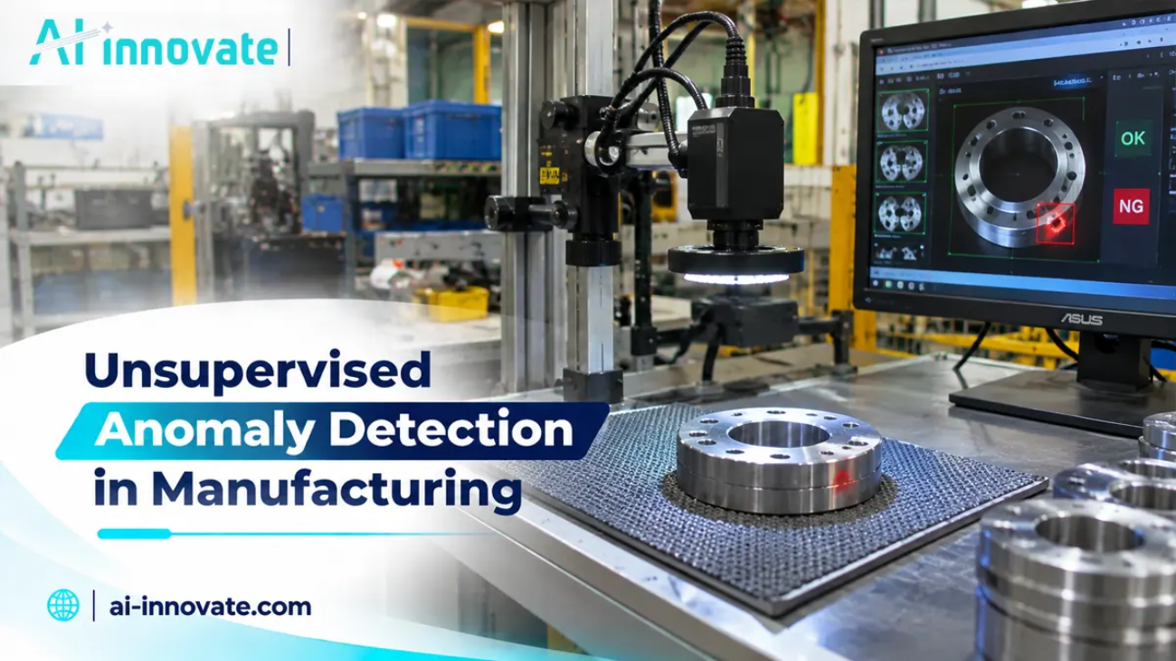
Unsupervised anomaly detection solves a fundamentally different problem. Instead of learning what specific defects look like, it learns what a normal, defect-free product looks like, and flags anything that deviates meaningfully from that learned pattern, whether or not that specific deviation has ever been seen before. This is not a theoretical distinction. In real manufacturing, defective samples are inherently scarce, the full range of possible defect types is rarely known in advance, and production lines evolve continuously, which means the defects a model needs to catch next month may not resemble anything in this month’s training data.

This guide covers why unsupervised anomaly detection has become a mainstream approach in industrial inspection, complementing the broader landscape covered in AI for defect detection, how the main technical methods actually work, what the field’s standard benchmark shows about real-world performance, and where this approach fits alongside supervised detection rather than replacing it outright.

Why Unsupervised Anomaly Detection Exists: The Labeled Data Problem

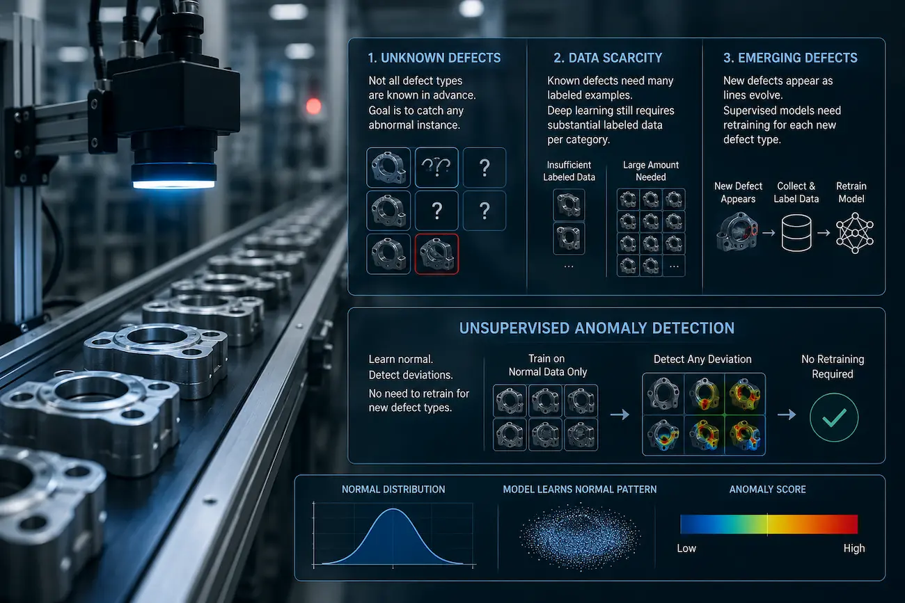
Three distinct problems push manufacturers toward unsupervised methods, and understanding them explains why this is not simply a workaround for insufficient data, but often the more appropriate approach entirely.

First, defect types frequently are not known beforehand. A manufacturer generally wants to catch any abnormal instance, not just the specific failure modes anticipated in advance, which is a poor fit for supervised models that depend on prior knowledge of exactly what they are looking for. Second, even when defect types are known, each one needs a meaningful number of labeled examples to train reliably, and most deep learning approaches still depend on substantial labeled volume per category despite advances in few-shot and one-shot learning, the same data scarcity challenge covered in AI machine vision for wafer defect detection, where synthetic data generation is used to work around a nearly identical constraint. Third, and often overlooked, new defect types emerge over time simply because production lines evolve, a resource change, a personnel change, a process drift, and a supervised model has to be retrained specifically on data representing that new defect type before it can catch it. Unsupervised models trained only to recognize deviation from normal do not carry this retraining burden in the same way, since they were never looking for a specific, named category of defect to begin with.
Why Unsupervised Anomaly Detection Exists

How Unsupervised Anomaly Detection Actually Works

The core mechanism is a form of one-class classification. During training, the model sees only normal, defect-free examples and learns to represent that normality as a statistical distribution, a learned feature space, or a reconstruction target, depending on the specific technique. At inference time, any input that falls meaningfully outside that learned boundary is scored as anomalous.

This is a genuinely different setup from standard object detection or classification, which require labeled examples of every category the model needs to recognize, defects included. Unsupervised anomaly detection needs zero defect labels for training. The training set contains only good samples, which is precisely what makes it a natural fit for manufacturing inspection, where defective samples are scarce by definition and represent exactly the class the model needs to catch.

The Main Technical Approaches

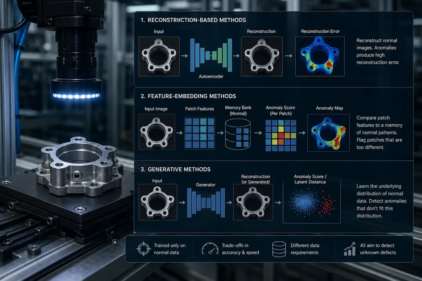
Unsupervised anomaly detection research has converged on a handful of distinct technical strategies, each with real trade-offs in accuracy, speed, and data requirements.

Reconstruction-Based Methods

Autoencoder architectures learn to compress and reconstruct normal images, and because they are trained exclusively on defect-free examples, they reconstruct anomalous regions poorly, producing a measurable reconstruction error that highlights where a defect likely sits. More advanced variants combine this with structural similarity loss or apply image inpainting techniques to improve robustness. DRAEM, a reconstructive-discriminative approach that trains against artificially generated anomalies using Perlin noise patterns, achieves a mean detection AUROC of 0.98 and localization AUROC of 0.973 on the standard industrial benchmark, approaching fully supervised results without ever training on a single real defect image.

Feature-Embedding Methods

Rather than reconstructing images, feature-embedding methods extract deep feature representations from normal samples and compare new samples against that learned feature space. PatchCore, one of the most widely adopted methods in this category, segments images into local patches, builds a memory bank of normal patch features, and flags anomalies based on how far a test patch’s features sit from anything in that memory bank. This patch-level, local approach to anomaly detection achieves strong detection and localization performance without requiring task-specific retraining for each new product line.

Generative Methods

Generative adversarial approaches, such as AnoGAN, learn the underlying distribution of defect-free texture patches directly, then detect anomalies by searching for the closest latent representation that could plausibly reproduce a given input. If no close match exists within the learned normal distribution, the input is flagged as anomalous. These methods were among the earliest unsupervised approaches applied to industrial inspection and remain an active area of ongoing research.
The Main Technical Approaches

The Benchmark That Defined This Field: MVTec AD

Nearly every unsupervised anomaly detection method gets measured against the same standard: MVTec AD, a real-world dataset comprising 5,354 images across 15 industrial object and texture categories, established specifically to give the field a rigorous, comparable benchmark for unsupervised detection and localization.

Its significance goes beyond convenience. Because the dataset provides pixel-precise ground truth annotations for every defect type across diverse, realistic industrial categories, it has become the reference point that any new method has to beat to be taken seriously. The benchmark family has since expanded to MVTec AD 2, which raises the difficulty bar further, and MVTec 3D-AD, extending unsupervised anomaly detection into three-dimensional geometric data captured by industrial 3D sensors, covering defects like scratches, dents, and deformations that manifest as geometric anomalies rather than pure surface texture changes.

Lorem ipsum dolor sit amet, consectetur adipiscing elit. Ut elit tellus, luctus nec ullamcorper mattis, pulvinar dapibus leo.

Add Your Heading Text Here

Published, comparative research evaluating multiple unsupervised methods head-to-head gives a clearer picture than any single paper’s reported numbers.

Method Approach Notable Strength
DRAEM Reconstruction with synthetic anomaly training 0.98 detection AUROC, 0.973 localization AUROC
PatchCore Patch-level feature memory bank Requires as few as 294 training images; strong localization accuracy
PaDiM Feature distribution modeling Fast training, well suited to rapid iteration across product categories
AnoGAN Generative adversarial modeling Early foundational approach; learns normal texture distribution directly

The practical takeaway from comparative evaluation is that unsupervised models are genuinely able to meet the performance expectations of real industrial use cases, while offering the flexibility of training without any predefined knowledge of what specific defect types to expect. PatchCore in particular has demonstrated that inference time, initially around 2 seconds per image, can be reduced to roughly 500 milliseconds by tuning the size of the training dataset, without materially sacrificing detection quality.

PatchCore in Practice: What Makes It the Practical Choice

PatchCore deserves particular attention because its practical characteristics solve real deployment problems, not just benchmark scores. It requires only a few hundred training images, in published evaluation as few as 294, a dramatically smaller data requirement than most supervised approaches demand even for a single defect category.

It does not require retraining when a new defect type appears, since it is not looking for a specific defect signature to begin with, only for meaningful deviation from the normal patch features it has already learned. And with sufficient dataset refinement, published results show it approaching perfect classification performance on standard benchmarks, closing much of the gap that once separated unsupervised methods from their supervised counterparts.

When Unsupervised Beats Supervised (and When It Doesn't)

Unsupervised anomaly detection is not universally the better choice, and understanding where it genuinely outperforms supervised approaches, and where it still falls short, matters for choosing the right method for a specific line.

  • Where unsupervised wins: catching defect types that have never been seen before, deploying on lines where defective samples are too rare to build a labeled dataset, and avoiding the retraining cycle every time a production change introduces a new failure mode.
  • Where unsupervised still struggles: the field’s own benchmark research is candid that no current method fully solves the problem, particularly at the low false-positive rates industrial deployment actually demands, and subtle, low-contrast defects that closely resemble normal texture variation remain genuinely difficult across nearly every published method.
  • Where a hybrid approach fits best: many production environments benefit from combining unsupervised detection as a broad first pass, catching genuinely novel anomalies, with supervised classification for well-characterized, high-volume defect types where labeled data already exists in abundance.

Getting Started: A Practical Path

  1. Collect a clean, representative set of normal-only images. The model’s entire understanding of “normal” comes from this dataset, so it needs to capture the real variation your line produces under normal operation, not just a handful of ideal samples.
  2. Choose a method based on your actual constraint. PatchCore for the best localization accuracy when defect location drives a repair decision; PaDiM when rapid iteration across many product variants matters more than squeezing out the last percentage point of accuracy.
  3. Set and validate your anomaly threshold carefully. The line between normal variation and a genuine anomaly is a tuning decision, not a fixed constant, and it should be validated against real production samples before going live, the same calibration discipline covered in real-time defect analysis.
  4. Monitor and periodically refresh the normal baseline. As legitimate process changes occur, materials, tooling, minor process adjustments, the definition of “normal” needs to evolve with them, or the model will begin flagging acceptable variation as anomalous.

How AI-Innovate Powers Unsupervised Anomaly Detection

Unsupervised anomaly detection addresses one of the most persistent constraints across every defect category this content has covered: the difficulty of building large labeled datasets for defects that are rare, evolving, or simply not yet known to exist.

AIxEye: Detection That Adapts as New Anomalies Emerge

AIxEye supports the kind of continuous, adaptive detection unsupervised approaches enable, catching genuine deviations from learned normal patterns rather than depending exclusively on a fixed catalog of previously labeled defect types.

AIxCore: Fast Enough Inference to Run Anomaly Detection at Line Speed

AIxCore handles the on-site processing that keeps anomaly detection fast enough for real production use, since the practical value of catching a novel defect drops sharply if the inference itself becomes a bottleneck on the line.

AIxAm: Extending Anomaly Detection Into Geometric and Dimensional Deviation

AIxAm applies the same underlying principle to 3D surface and geometric inspection, comparing captured part geometry against a learned normal baseline to catch dimensional anomalies that a purely 2D, texture-based approach was never built to see.

Final Thoughts

Unsupervised anomaly detection reframes the defect detection problem in a way that matches how manufacturing actually works: defective samples are scarce, new failure modes appear without warning, and waiting to accumulate enough labeled examples of a new defect type before a model can catch it is often not acceptable. Learning what normal looks like, and flagging genuine deviation from it, sidesteps that constraint entirely.
The manufacturers getting the most value from this approach are not treating it as a replacement for supervised detection everywhere. They are using it where it is genuinely suited, catching the unknown and the rare, while keeping supervised classification for well-characterized, high-volume defect categories where labeled data already exists. That combination, rather than a single universal method, is what closes the gap between what a model was trained to expect and what a real, continuously evolving production line actually produces.

Frequently Asked Questions

What is the difference between supervised and unsupervised anomaly detection?

Supervised detection trains on labeled examples of specific defect types and can only recognize defects it was explicitly trained to identify. Unsupervised anomaly detection trains only on normal, defect-free samples and flags any meaningful deviation from that learned pattern, including defect types it has never encountered before.

Unsupervised methods are especially valuable when defect types are not fully known in advance, when defective samples are too scarce to build a reliable labeled dataset, or on production lines that evolve frequently enough that a supervised model would need constant retraining to keep up with new failure modes.

Requirements vary by method, but published research on PatchCore, one of the most widely used approaches, shows strong performance with as few as 294 training images, all of them normal, defect-free samples, since no labeled defect examples are required at all.

 MVTec AD is the standard benchmark dataset for unsupervised anomaly detection, comprising 5,354 real-world images across 15 industrial categories with pixel-precise defect annotations. It is the reference point nearly every new unsupervised method is measured against, and its extensions now cover harder 2D scenarios and 3D geometric anomaly detection.

 Not entirely. Research in this area is candid that current unsupervised methods have not fully solved the problem, particularly for subtle defects at the low false-positive rates real production lines require. Most effective deployments combine unsupervised detection for novel or rare anomalies with supervised classification for well-characterized, high-volume defect types.

 Performance varies by method and configuration, but published results on PatchCore show inference time reduced from around 2 seconds to approximately 500 milliseconds per image through dataset size tuning, fast enough for real production line deployment in most applications.

Ai-Innovate uses only high-quality sources, including peer-reviewed studies, to support the facts within our articles.

  1. Rippel, O., Mertens, P., & Merhof, D. (2023). Anomaly detection for industrial quality assurance: A comparative evaluation of unsupervised deep learning models. Computers & Industrial Engineering. https://www.sciencedirect.com/science/article/pii/S0360835223000694


  2. Bergmann, P., Fauser, M., Sattlegger, D., & Steger, C. (2019). MVTec AD: A Comprehensive Real-World Dataset for Unsupervised Anomaly Detection. Proceedings of the IEEE/CVF Conference on Computer Vision and Pattern Recognition. https://arxiv.org/pdf/2309.06884
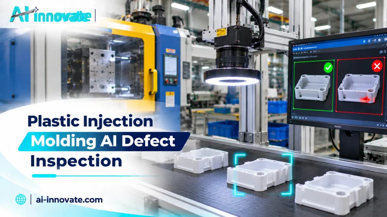
Plastic Injection Molding AI Defect Inspection

Plastic Injection Molding AI Defect Inspection

A 0.1mm sink mark on a black bumper. A weld line on a transparent housing. A flash burr on a connector body. Each one is the kind of defect a quality engineer can spot instantly in a lab under the right light, and loses just as easily to fatigue on a twelve-hour shift running at 240 parts per minute. Injection molding produces an unusually specific, unusually visual category of defects, and catching them reliably at production speed has always been a genuine limitation of manual inspection, not a matter of inspector skill.

The results when AI vision closes that gap are not aspirational numbers. BMW’s Leipzig plant reported a 34 percent reduction in scrap rates after integrating AI vision into bumper production, and that figure sits comfortably within the 20 to 40 percent scrap reduction most injection molding deployments report once the system is properly tuned.

This guide covers the specific defect catalog injection molding produces, building on the broader ground AI quality control solutions for plastic manufacturing covers, how AI vision detects each one, where the camera and lighting actually belong, and what the economics look like once a system is running.

Why Injection Molding Produces Such a Distinct Set of Defects

Injection molding runs through a six-phase cycle, and understanding it explains why the defect catalog looks the way it does, a process-to-defect link that mirrors what common causes of defects in manufacturing shows across other industries: most escaped defects trace back to a specific, identifiable point in the process rather than a random occurrence. Resin drying removes moisture that would otherwise cause splay.

Plasticization melts and homogenizes the material charge. Injection fills the cavity volumetrically in a matter of seconds. Hold pressure packs out volumetric shrinkage after the cavity is full. Cooling solidifies the part to ejection temperature. Each phase has its own tight control tolerances, and a deviation in any one of them, melt temperature drifting by a couple of degrees, fill time shifting by fractions of a second, hold pressure dropping a percentage point, produces a specific, visually distinct defect in the finished part. That tight coupling between process parameter and visible defect is exactly what makes this category so well suited to AI vision: the defects are concrete, repeatable, and tied to a bounded set of part geometries rather than open-ended visual variation.

The Injection Molding Defect Catalog

Each defect type traces back to a specific point in the molding cycle, and detection approaches vary accordingly.

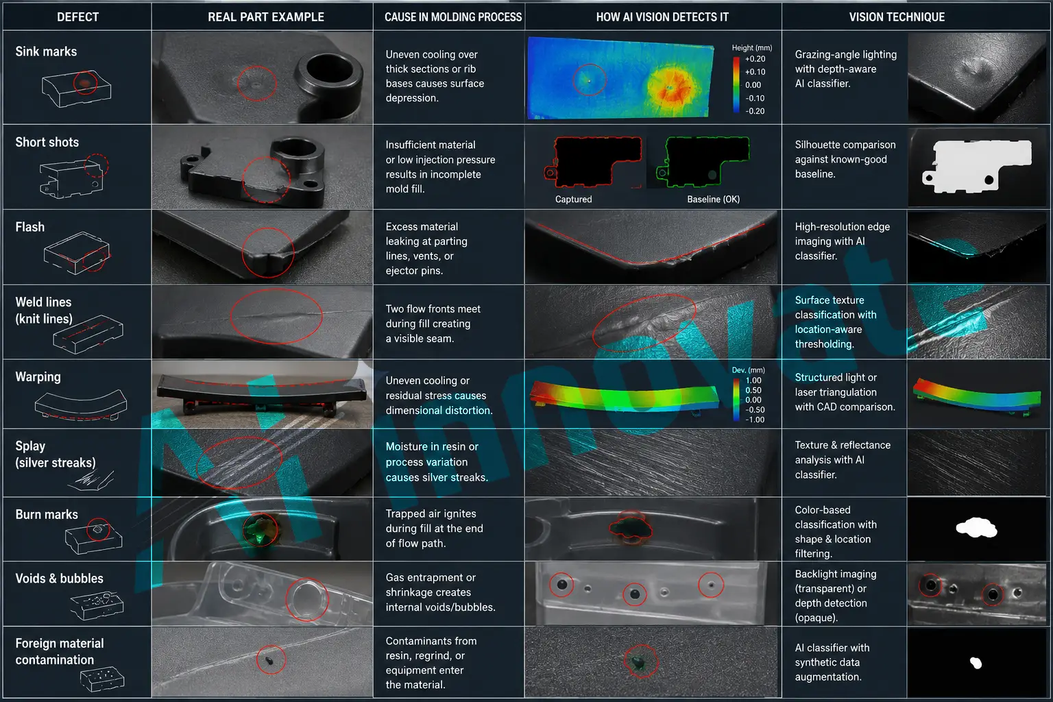
  •   Sink marks. Small surface depressions from uneven cooling, typically over thick wall sections or rib bases. Sub-millimeter sink marks, as shallow as 0.1mm, are the hardest class to catch by eye, particularly on dark or textured surfaces, but AI vision detects them reliably with grazing-angle lighting and a depth-aware classifier.
  •   Short shots. Incomplete mold fill leaving a part with missing geometry, always a reject. Detection by silhouette comparison against a known-good baseline is straightforward, which is why short shots are typically the first defect class deployed on a new line.
  •   Flash. Excess material at parting lines, vents, or ejector pin locations. Detection requires sub-millimeter edge resolution along the entire parting line, a task where rule-based vision struggles because the parting line varies subtly across mold tools and material lots, but a trained AI classifier handles well.
  •   Weld lines (knit lines). Visible seams where two flow fronts meet during fill, always present but sometimes prominent enough to be a cosmetic reject, especially on transparent or translucent parts. Detection uses a surface texture classifier with location-aware thresholding, since some weld lines are acceptable in non-visible regions.
  •   Warping. Dimensional distortion from uneven cooling or residual stress. This is one of the cases where pure 2D vision falls short; warping generally needs structured-light or laser triangulation paired with a dimensional comparison against the CAD model.
  •   Splay (silver streaks). Streaks caused by moisture in the resin or process variation, a cosmetic reject on visible surfaces that often signals an upstream resin handling issue worth investigating, not just a part-level defect.
  •   Burn marks. Dark discolored regions where trapped air ignites during fill, typically at the end of long flow paths, and always a reject. Detection uses a color-based classifier with shape and location filtering to distinguish burns from ordinary texture variation.
  •   Voids and bubbles. Internal pockets on transparent parts, detected with backlight imaging, or surface-level depressions on opaque parts, which require depth-aware detection.
  •   Foreign material contamination. Particulate, fiber, or color contamination introduced during upstream resin handling. Because real contamination samples are rare and highly varied, synthetic data augmentation is particularly valuable for training a reliable classifier here.

Cavity-Pressure Prediction vs Vision Confirmation: Two Complementary Systems

Vision inspection catches defects after a part is ejected. A second, complementary approach catches many of the same defects before the part ever leaves the mold. Cavity pressure is the single most information-dense process signal available on an injection molding press: it encodes the entire fill and pack history of that specific shot, and a deviation from the validated baseline is often the earliest available indicator that a defect is forming. Neural network models trained on in-mold temperature and cavity pressure data can predict outcomes like part mass, wall thickness, and tensile strength directly from that in-cycle sensor trace, while the part is still inside the mold.

These two systems are complementary, not redundant. Cavity-pressure prediction catches process-origin defects before they even become finished parts. Vision confirms the prediction after ejection and catches anything the process model missed, providing the geometric ground truth needed to validate and improve that model over time. The most common mistake facilities make is running these two systems independently, which means a sink-mark increase on one cavity generates a vision alert and a separate process alert that nobody automatically connects, turning a root-cause investigation into a multi-day manual correlation exercise instead of an answer available in seconds.

The Cost of Catching a Defect Late

Where in the process a defect gets caught changes its cost by an order of magnitude, sometimes two. A defect caught at the press costs roughly the value of one part and one shot’s worth of cycle time. The same defect discovered at assembly, where it causes a downstream failure or requires disassembly and rework, costs five to ten times as much. Caught only at the customer, as a warranty return or field failure, the cost multiplies again to fifty to one hundred times the press-side figure.

This is precisely why the hidden cost of missed defects compounds so severely in injection molding specifically: manual visual inspection typically covers only around 5 percent of production volume, which means a defect affecting even 3 percent of shots can produce thousands of defective parts in a single shift before anyone notices, and by the time it does, most of those parts have already moved well past the point where catching them was cheap.

Where to Place the Inspection Camera

Camera placement involves real trade-offs, and the right choice depends on part value, cycle speed, and the cost of downstream handling.

Press-Side, Immediately After Ejection

Catches defects before any handling damage occurs and lets the press control system flag and divert a bad part automatically. The drawback is thermal stress on the camera, press vibration, and constrained camera angles, which makes this placement worth the added engineering investment mainly for high-cycle, high-cost parts where catching a reject before it leaves the press meaningfully reduces downstream waste.

Post-Conveyor, Before Downstream Processing

The most common placement and the right starting point for most lines. It offers a stable thermal environment, multiple camera angles, and full 360-degree inspection feasibility, though defective parts may have already been handled or stacked by the time they reach this point.

Post-Trim or Post-Secondary Operation

Useful when secondary operations like degating, trimming, or bonding introduce their own distinct defect classes. Running inspection both before and after each secondary step helps localize exactly which operation is responsible when a new defect appears.

Lighting Considerations for Injection Molded Parts

Most injection molding inspection failures trace back to lighting design, not algorithm limitations. Black plastic, glossy surfaces, and complex part geometry all demand deliberate lighting choices rather than a single generic setup.

  •   Diffuse dome lighting for highly reflective or glossy surfaces.
  •   Grazing-angle structured lighting for sink marks, dents, and other subtle surface defects.
  •   Backlighting for transparent or translucent parts, revealing voids and inclusions.
  •   Coaxial lighting for highly specular surfaces where reflections need to be controlled.
  •   Multi-spectral imaging for contamination that is color-similar to the base material and invisible in standard RGB.

Training Data and the Rare Defect Problem

Modern AI vision platforms reach production-grade accuracy on injection molding defect classes with as few as 5 to 20 real defective images per class, which surprises many teams expecting to need thousands of examples. The real constraint is not raw image volume but the quality and diversity of those images within the actual production envelope. For genuinely rare defect classes, those occurring less than once per 10,000 parts, synthetic defect generation closes the gap without waiting months to accumulate enough natural samples, which matters enormously for defect types like foreign material contamination that are both rare and highly variable in appearance.

Real-World Results: What Deployments Actually Show

Typical injection molding lines run scrap rates of 1 to 5 percent on stable production, and AI vision deployments consistently report a 20 to 40 percent reduction in that baseline scrap rate. On a line producing 10 million parts a year at 50 cents per part, a 30 percent reduction against a 3 percent baseline scrap rate recovers roughly $45,000 annually, a figure that scales directly with line volume and part cost. Most inspection systems pay back within a year on typical production volumes, and on automotive Tier-1 part programs, payback frequently lands under six months.

Getting Started: A Practical Deployment Timeline

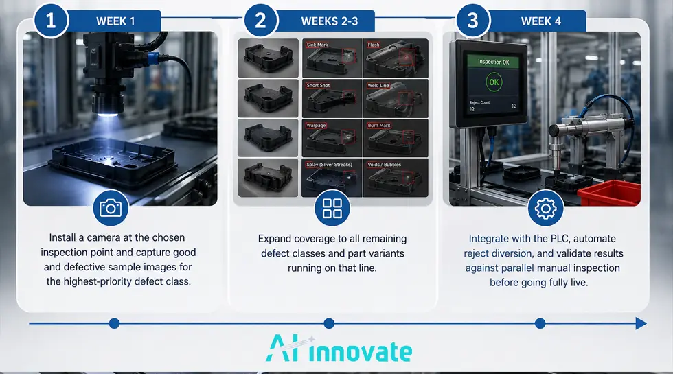
  1.   Week 1. Install a camera at the chosen inspection point and capture good and defective sample images for the highest-priority defect class.
  2.   Weeks 2-3. Expand coverage to all remaining defect classes and part variants running on that line.
  3.   Week 4. Integrate with the PLC, automate reject diversion, and validate results against parallel manual inspection before going fully live.
Getting Started A Practical Deployment Timeline

How AI-Innovate Powers Injection Molding Defect Inspection

Injection molding compresses a lot of inspection difficulty into a single part: sub-millimeter defects, glossy and dark surfaces that punish generic lighting setups, dimensional distortion that pure 2D imaging cannot catch, and rare contamination classes that real production data alone would take years to accumulate examples of.

AIxEye: Real-Time Detection Across the Full Defect Catalog

AIxEye performs the visual inspection that covers the injection molding defect catalog end to end, sink marks, short shots, flash, weld lines, splay, burn marks, and contamination, adapting detection criteria to the specific part geometry, material, and color running on a given line rather than applying one fixed threshold across every mold tool.

AIxAm: Synthetic Data for Rare and Variant-Specific Defects

AIxAm addresses the training data gap that matters most in injection molding: generating synthetic examples for defect classes that occur too rarely in real production to build a large natural dataset, and helping propagate a known defect class across part color and material variants without re-collecting samples for every combination a single mold tool produces.

AIxCore: Edge Processing Fast Enough for Press-Side Inspection

AIxCore handles the on-site inference that makes press-side inspection viable even at fast cycle times, processing each part locally so a reject decision can trigger automatic diversion before the part moves further down the line, without depending on a network round trip that press-side thermal and vibration conditions would make unreliable anyway.

Final Thoughts

Plastic injection molding produces a defect catalog that is unusually well suited to AI vision: concrete, visually distinct, tightly coupled to specific process parameters, and expensive to catch late rather than at the press. Sink marks, short shots, flash, warping, and the rest of the catalog each trace back to a specific point in the six-phase molding cycle, which is exactly why detection approaches tuned to each defect type outperform a single generic inspection setup.

The facilities getting the strongest results are not just bolting a camera onto the line. They are pairing vision inspection with cavity-pressure process data where possible, placing cameras and lighting deliberately rather than defaulting to whatever fits, and treating rare defect classes as a data problem synthetic generation can solve rather than a gap to wait out. With scrap reduction in the 20 to 40 percent range and payback typically under a year, the economics of getting this right are no longer a hard case to make.

Frequently Asked Questions

What defects can AI vision detect on injection molded parts?

AI vision systems detect the full range of injection molding defects: sink marks, short shots, flash, weld lines, warping, splay, burn marks, voids, and foreign material contamination. Sub-millimeter sink marks down to 0.1mm can be detected reliably with proper lighting and camera resolution.

Sub-100ms inference per part is standard for production AI vision systems, comfortably supporting cycle times under one second per part on most molding lines. Image capture, particularly lighting and motion stability, is typically the bottleneck rather than inference speed.

Most injection molding deployments report scrap reduction in the 20 to 40 percent range, with payback periods of 3 to 9 months on typical line volumes. BMW’s Leipzig plant reported a 34 percent scrap rate reduction after integrating AI vision into bumper production.

Modern AI vision platforms reach production-grade accuracy with as few as 5 to 20 real defective images per defect class on most applications. Synthetic data generation can supplement genuinely rare defect classes occurring at roughly 1 per 10,000 parts or less.

Post-conveyor placement is the right starting point for most lines, offering a stable thermal environment and full inspection angle coverage. Press-side placement catches defects before handling damage but requires managing thermal stress and vibration, and is generally worth that investment for high-cycle, high-cost parts.

Not entirely. Vision inspection catches defects after a part is ejected, while cavity-pressure sensors can predict certain process-origin defects, like those tied to mass, wall thickness, or tensile strength, before the part is even out of the mold. The two approaches are complementary, with vision providing the geometric ground truth that process models need to stay accurate.

Ai-Innovate uses only high-quality sources, including peer-reviewed studies, to support the facts within our articles.

  1. Overview.ai. (2026). Plastic Injection Molding AI Defect Inspection: A Practical Guide. https://www.overview.ai/blog/plastic-injection-molding-ai-defect-inspection/
  2. Niobia AI. (2026). Injection Molding AI: Cavity-Pressure + Vision, Zero-Escape Defect Control. https://niobia.ai/applications/injection-molding
AI Machine Vision System for Wafer Defect Detection

AI Machine Vision System for Wafer Defect Detection

A modern transistor operates at sub-5 nanometer scale, smaller than a virus. At that geometry, a single scratch, particle, or misaligned pattern on a silicon wafer does not just create a cosmetic flaw. It can reject an entire die, cascade into significant yield loss, and cost a fab millions of dollars, all from a defect the human eye was never going to reliably catch under a microscope, shift after shift.

That is the reality semiconductor manufacturing has been racing to address, and AI-powered machine vision has become the clearest path forward.
The challenge is not simply pointing a camera at a wafer. Semiconductor defect detection has to work at a precision manual optical inspection cannot sustain, across increasingly complex multi-layer structures, in a cleanroom environment where every second of inspection time carries real production cost.

This guide covers what actually goes into an AI machine vision system for wafer defect detection: the defect types involved, the architectures used to catch them, how researchers are solving the field’s hardest data problem, and what published, peer-reviewed results actually show.

Why Wafer Inspection Is Different From Other Manufacturing Defect Detection

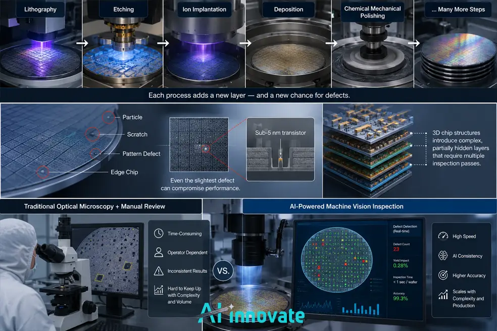
Semiconductor wafers are built through dozens of tightly controlled steps, lithography, etching, ion implantation, deposition, each adding a new layer and a new opportunity for a defect to appear. Unlike most manufactured products, a wafer’s defects are not just surface-level cosmetic issues.

Shrinking transistor geometries mean even the slightest surface anomaly can compromise device performance, and the shift toward 3D chip structures adds complex, partially hidden layers that each require their own inspection pass.

Traditional optical microscopy paired with manual expert review has handled this for decades, but as chip designs grow more sophisticated and production volumes climb, that approach has become both too slow and too inconsistent to keep pace.

What Defects Actually Occur in Wafer Fabrication

Wafer defects fall into a consistent set of categories that AI vision systems are trained to recognize, each tied to a different stage or mechanism in the fabrication process.

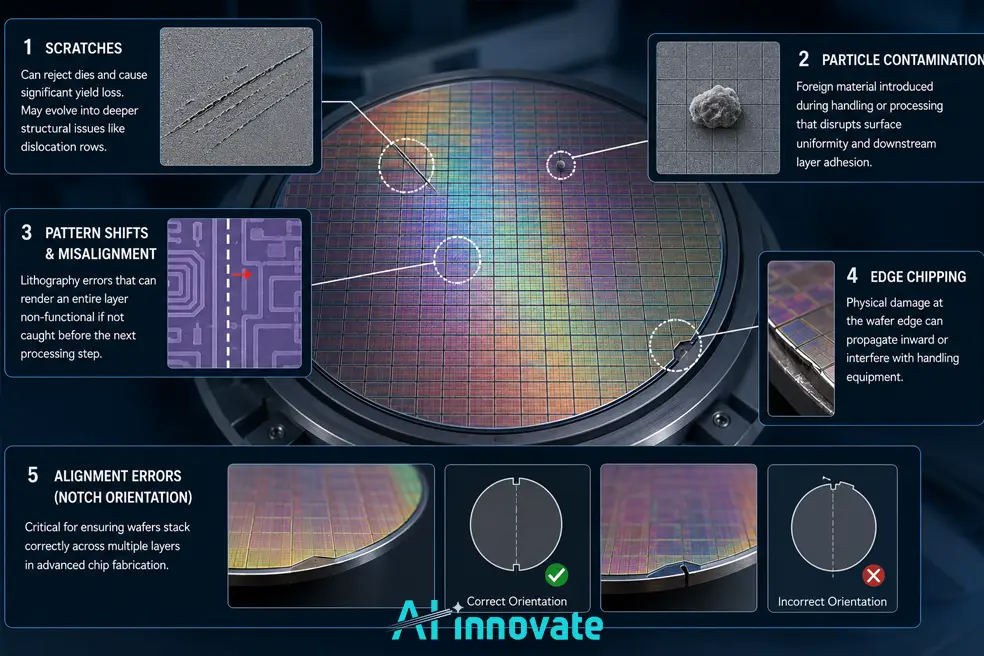
  • Scratches, among the most critical defect types in wafer fabrication, capable of rejecting dies and causing substantial yield loss even when shallow, and sometimes evolving into deeper structural issues like dislocation rows if left undetected.
  • Particle contamination, foreign material introduced during handling or processing that disrupts surface uniformity and downstream layer adhesion.
  • Pattern shifts and misalignment, errors introduced during lithography that can render an entire layer non-functional if not caught before the next processing step.
  • Edge chipping, physical damage at the wafer edge that can propagate inward or interfere with handling equipment.
  • Alignment errors, including notch orientation issues, which are critical for ensuring wafers stack correctly across the many layers of modern chip fabrication.
What Defects Actually Occur in Wafer Fabrication

How AI Vision Systems Detect Wafer Defects

Optical Scanning and Image Acquisition

Wafer inspection begins with optical scanning microscopy, capturing high-resolution images of the wafer surface as part of the same broader discipline of machine vision for defect detection applied at semiconductor scale.

A machine vision system built specifically for this purpose, using an optical scanning setup paired with an AI algorithm based on the Mask R-CNN architecture, has been demonstrated on microscopic images of wafers containing Micro Electro-Mechanical Systems, silicon photonics, and superconductor devices at different fabrication stages, with the researchers reporting accuracy and detection speed promising enough for real cleanroom application.

Object Detection Architectures

Beyond Mask R-CNN, YOLO-based object detection has become one of the most widely applied architectures for wafer defect detection, valued for its single-pass speed and accuracy, which suits the real-time demands of high-volume fabrication lines. Because surface defects like scratches or particles are often tiny and appear in visually complex, multi-layered backgrounds, successive YOLO generations have specifically improved detection of small, low-contrast objects, a capability that matters enormously at the scale modern wafers are inspected.

Multi-Layer, Multi-Stage Inspection

Because a wafer accumulates layers throughout fabrication, inspection is not a single checkpoint but a distributed process embedded across the workflow, from unpatterned wafer inspection immediately after slicing and polishing through patterned wafer inspection following each lithography step, a layered inspection challenge not unlike the imaging trade-offs covered in 2D vision vs 3D vision systems for inspection.

This layered inspection approach is what lets defects get caught close to where they originate, rather than only surfacing once a wafer reaches final test, by which point far more value has already been added to a potentially defective unit.

Solving the Data Scarcity Problem With Synthetic Training Data

The single biggest obstacle to AI-based wafer inspection is not algorithm performance. It is data. Collecting sufficient annotated real-world defect images is prohibitively expensive and disruptive to a live production line, and rare or emerging defect types are often underrepresented or entirely absent in existing datasets, limiting how well a model can generalize.

Recent peer-reviewed research addresses this directly with a fully synthetic-data-driven approach. Researchers built a high-fidelity 3D simulation environment in Blender to procedurally generate thousands of labeled wafer images featuring scratch-type defects under varying lighting, texture, and geometric conditions, then trained YOLO object detection models exclusively on that synthetic data, with no real-world annotated training images at all.

When evaluated against real wafer images captured on a physical optical inspection system, models trained purely on synthetic data achieved F1 scores of 1.00 for wafer presence classification and F1 scores exceeding 0.96 for scratch defect localization. This is a meaningful result: it demonstrates that the field’s most persistent data bottleneck can be worked around without the cost and disruption of large-scale manual annotation.

Real-World Performance: What the Research Shows

The same study benchmarked three YOLO architectures, YOLOv8m, YOLOv10m, and YOLOv11m, across two detection tasks: wafer presence and scratch defect localization.

Model Wafer Presence F1 Scratch Detection F1
(Best Epoch)
Notes
YOLOv8m 1.00 0.9821 Peaked early, showed overfitting with extended training
YOLOv10m 0.9744 0.8859 Highly sensitive to training duration, least consistent
YOLOv11m 1.00 0.9685 Most robust, best resistance to overfitting

The pattern that emerges is consistent with broader industrial defect detection research: wafer presence, a coarse binary classification task, is solved reliably by nearly every architecture tested, while fine-grained scratch localization, which depends on small, low-contrast, pixel-level features, is meaningfully harder and separates the architectures clearly, the same accuracy-versus-speed trade-off explored in real-time defect analysis more broadly. YOLOv11m’s combination of strong accuracy and resistance to overfitting made it the most reliable choice for the harder task in this research.

Where AI Vision Fits Across the Fabrication Process

AI-powered inspection is not confined to a single stage of chip production. It extends across the full manufacturing flow.

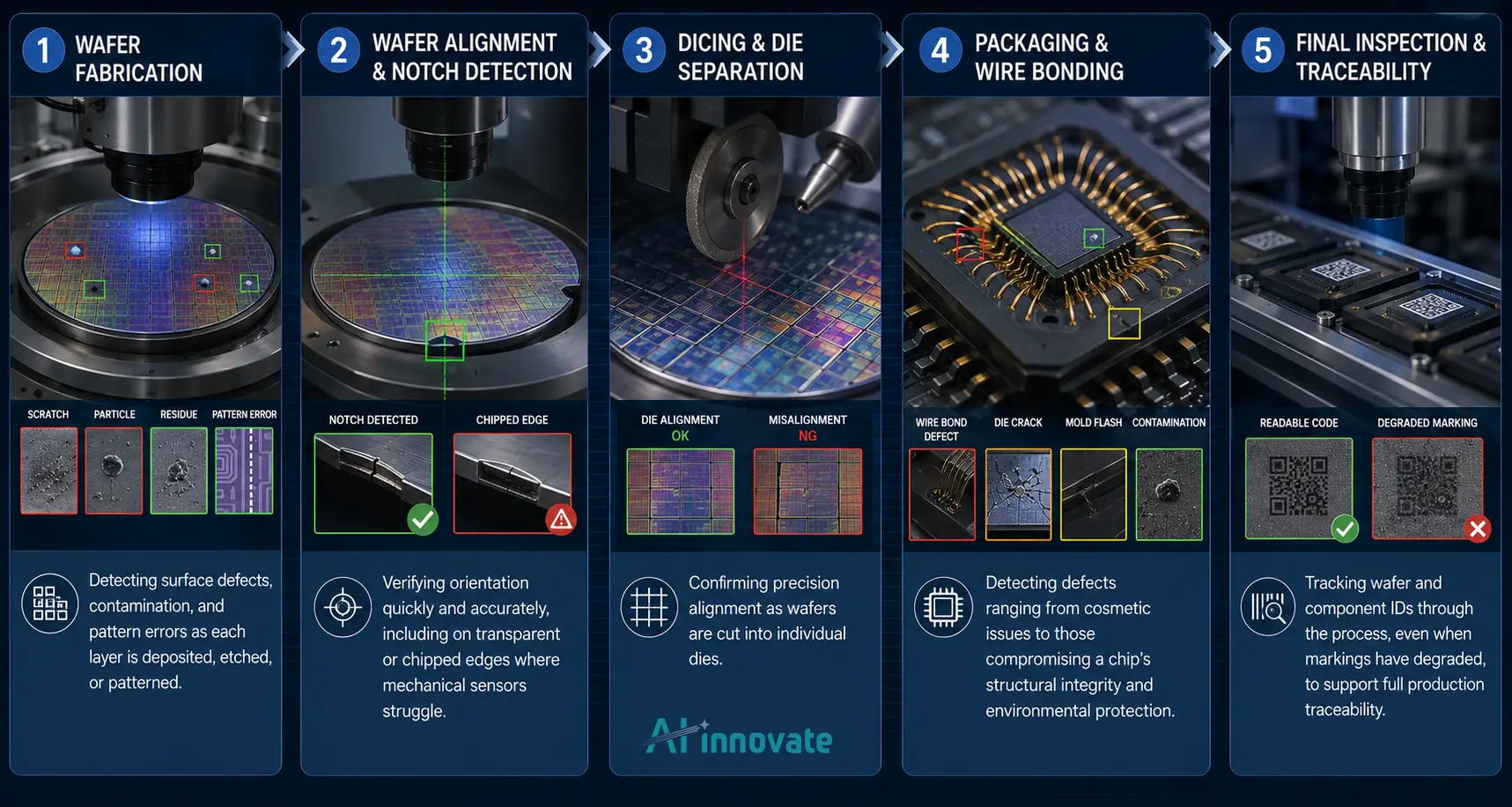
  1.   Wafer fabrication. Detecting surface defects, contamination, and pattern errors as each layer is deposited, etched, or patterned.
  2.   Wafer alignment and notch detection. Verifying orientation quickly and accurately, including on transparent or chipped edges where mechanical sensors struggle.
  3.   Dicing and die separation. Confirming precision alignment as wafers are cut into individual dies.
  4.   Packaging and wire bonding. Detecting defects ranging from cosmetic issues to those compromising a chip’s structural integrity and environmental protection.
  5.   Final inspection and traceability. Tracking wafer and component IDs through the process, even when markings have degraded, to support full production traceability.
Where AI Vision Fits Across the Fabrication Process

How AI-Innovate Supports Semiconductor Wafer Inspection

Wafer inspection sits at the extreme end of machine vision difficulty: nanometer-scale defects, multi-layer structures, cleanroom throughput demands, and a data scarcity problem that makes conventional training approaches genuinely difficult. It is exactly the kind of environment where a purpose-built inspection platform earns its value.

AIxEye: Precision Detection for Microscopic Defects

AIxEye delivers the real-time visual inspection capability at the core of wafer-level quality control, trained to recognize the scratch patterns, contamination signatures, and pattern irregularities that matter at semiconductor scale, adapting detection criteria to the specific fabrication stage and defect profile of a given line rather than applying one generic threshold across every layer.

AIxAm: Synthetic Data for the Industry's Hardest Data Problem

AIxAm addresses precisely the data bottleneck the published research above confirms is the field’s biggest constraint. Generating synthetic training examples for rare or emerging defect types means a model can learn to recognize a failure mode reliably without requiring the months, or years, it would take to accumulate enough real annotated examples from production alone.

AIxCore: Edge Processing for Cleanroom-Speed Inspection

AIxCore handles the on-site inference that keeps wafer inspection fast enough to matter in a high-throughput fabrication environment, processing decisions locally rather than depending on a round trip to the cloud, the same edge AI deployment principles that apply to real-time inspection across manufacturing generally, which matters enormously when inspection results need to gate the next processing step in real time.

Final Thoughts

AI machine vision for wafer defect detection has matured into a genuinely capable technology, with peer-reviewed research now demonstrating that even models trained entirely on synthetic data can achieve near-perfect accuracy on real wafer images, directly addressing the data scarcity problem that has historically limited how far AI could be pushed in this field.
The manufacturers and fabs seeing the strongest results are not simply pointing a camera at a wafer and hoping a generic model catches what matters. They are matching detection architecture to defect type, recognizing that coarse presence detection and fine-grained scratch localization are genuinely different problems with different reliability profiles, and increasingly turning to synthetic data generation to train for the rare defect types that real production data alone would take years to accumulate. At a scale where a single undetected scratch can cost millions in yield loss, that level of deliberate engineering is not optional. It is the baseline for staying competitive.

Frequently Asked Questions

What types of defects does AI vision detect on semiconductor wafers?

AI vision systems detect scratches, particle contamination, pattern shifts and misalignment from lithography, edge chipping, and alignment or notch orientation errors, covering defects introduced at nearly every stage of wafer fabrication from slicing through final packaging.

Published peer-reviewed research has reported F1 scores of 1.00 for wafer presence detection and F1 scores exceeding 0.96 for fine-grained scratch defect localization, using YOLO-based object detection models, indicating high reliability for both coarse and detailed inspection tasks.

Yes. Recent research demonstrates that YOLO models trained exclusively on synthetic wafer images generated through 3D simulation can achieve strong performance on real wafer images, directly addressing the scarcity and cost of collecting large volumes of labeled real-world defect data.

Wafer presence is a coarse binary classification task where the wafer occupies most of the image frame with a strong geometric signature. Scratch detection involves small, low-contrast, pixel-level features whose visibility depends heavily on lighting and surface micro-texture, making it a meaningfully harder detection problem.

Both Mask R-CNN and YOLO-based architectures have been demonstrated in published research for wafer defect detection. Mask R-CNN has been applied to microscopic wafer imagery for defect segmentation, while YOLO variants are widely used for their speed and accuracy in real-time, high-volume inspection scenarios.

AI vision is used throughout fabrication, including wafer surface inspection after each processing layer, wafer alignment and notch detection, dicing precision verification, packaging and wire bond inspection, and traceability tracking across the full production flow.

Ai-Innovate uses only high-quality sources, including peer-reviewed studies, to support the facts within our articles.

  1. Morits, D., Piton, M. R., & Laakko, T. (2023). AI Machine Vision System for Wafer Defect Detection. In Industrial Artificial Intelligence Technologies and Applications (pp. 73-80). River Publishers. https://doi.org/10.1201/9781003377382-5
  2. Sánchez Peñaloza, R. J., Moghadam, A., & Davoudi Kakhki, F. (2026). Vision-Based Wafer Inspection in Semiconductor Manufacturing: A Case Study on Scratch Defect Detection Using Synthetic Data and YOLO Models. International Journal of Data Science and Analytics, 22, 78. https://doi.org/10.1007/s41060-026-01034-8
  3. Jeganathan, B. (2025). Machine Learning and Deep Learning in Wafer Defect Detection: Current State and Future Directions. Current Journal of Applied Science and Technology, 44(12), 1–14.
    https://doi.org/10.9734/cjast/2025/v44i124637
  4. Morits, D., Rizzo Piton, M., & Laakko, T. (2022). AI Machine Vision System for Wafer Defect Detection. In Industrial Artificial Intelligence Technologies and Applications (pp. 73–80). River Publishers.
    https://doi.org/10.13052/rp-9788770227902
  5. Lee, H. C. (2026). AI System for Wafer Defect Detection. U.S. Patent No. 12,638,838 B2. U.S. Patent and Trademark Office.
    https://www.goveda.com/patent/US-12638838-B2
  6. Robovision. (2024). AI-Based Wafer Defect Inspection: An Accuracy and Efficiency Boost.
    https://robovision.ai/blog/ai-based-wafer-defect-inspection-an-accurracy-and-efficiency-boost
AI-Powered Defect Detection in Rubber Tire Manufacturingwebp

AI-Powered Defect Detection in Rubber Tire Manufacturing

A tire is not a product where “close enough” is acceptable. It is the only part of a vehicle that touches the road, and a defect that escapes inspection, a sidewall crack, a mold-related imperfection, a hidden air bubble, does not just risk a warranty claim. It risks a safety failure. That is exactly why tire manufacturing has some of the strictest quality requirements in industrial production, and exactly why manual inspection alone has become harder to trust as production speeds and design complexity both keep rising.

The core difficulty is not that tire defects are impossible to see. Most begin as small, subtle anomalies during rubber preparation, curing, trimming, or finishing. The difficulty is finding them consistently across thousands of tires a shift, on a curved, textured, low-contrast surface that behaves nothing like the flat, uniform materials most inspection systems were originally designed for. AI-powered visual inspection has become the industry’s answer to that consistency problem, and it works differently from how most people assume automated inspection works.

This guide covers where tire defects actually originate, why tires are a genuinely hard inspection target, how AI systems handle that difficulty in practice, and what the technology actually delivers once deployed.

Why Tire Inspection Is Uniquely Difficult

Unlike flat sheet metal or glass, a tire is curved, textured, and structurally complex, with a tread pattern, sidewall markings, and material transitions that make consistent imaging genuinely hard. Rubber itself is a difficult surface for machine vision: it is low-contrast, prone to surface reflections under certain lighting, and varies naturally from tire to tire even when every one is within spec.

The same defect can look visually different on two different tires depending on curvature, angle, and surface texture, which is precisely where older rule-based inspection systems, built around fixed thresholds, tend to struggle. Add rising production speeds and increasingly complex tire designs, and manual inspection faces a scale problem that has nothing to do with inspector skill and everything to do with the sheer volume and subtlety involved.

Why Tire Inspection Is Uniquely Difficult

Where Tire Defects Actually Begin

Manufacturing defects rarely announce themselves as catastrophic failures. In almost every case, they start as minor anomalies introduced somewhere earlier in production, during rubber mixing, molding, curing, trimming, or finishing.

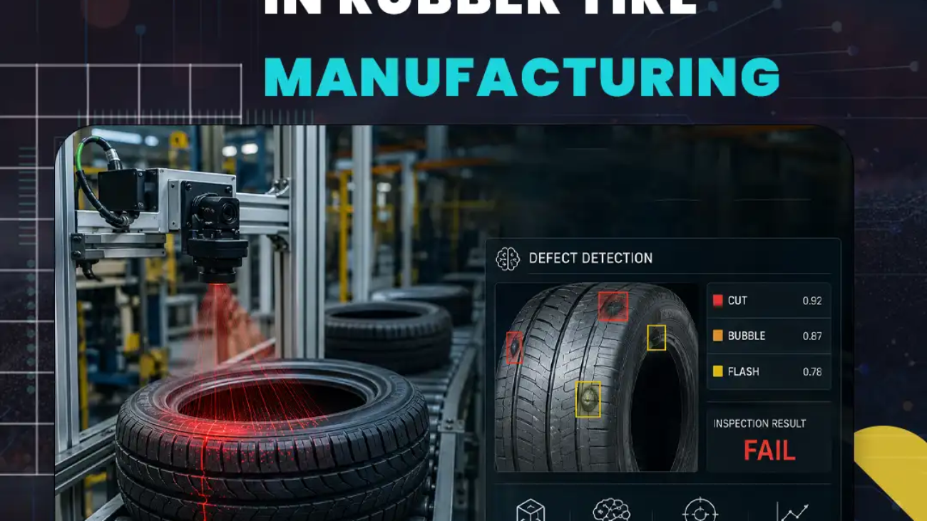
  • Sidewall cracks, often linked to material stress or curing inconsistencies
  • Surface cuts, typically introduced during handling or trimming
  • Air bubbles and blisters, trapped during the molding or curing process
  • Tread inconsistencies, affecting pattern accuracy and performance
  • Material contamination, foreign particles introduced during mixing
  • Mold-related imperfections, tied to wear or damage in the mold itself
  • Flashing defects, excess rubber left at mold parting lines
  • Surface texture abnormalities, deviations from expected finish and grain


The challenge is not that any single defect type is exotic or hard to define. It is catching all of them, consistently, across the volume a modern tire plant produces every shift.

How AI Tire Inspection Actually Works

Modern AI-powered tire inspection combines several distinct technologies, and understanding how they fit together explains why this approach succeeds where older 2D systems struggled.

3D Surface Acquisition

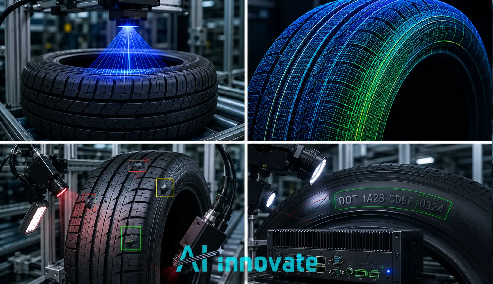
Rather than relying on flat 2D imaging, advanced systems use laser profilometry to generate a precise three-dimensional reconstruction of the tire’s surface. This captures micrometric variations, the kind of subtle folds, material inconsistencies, and improper junctions, that are effectively invisible to a standard 2D camera working with a curved, low-contrast rubber surface.

AI-Based Defect Classification

AI algorithms analyze the 3D surface model to detect and classify specific defect types. This is where the underlying approach differs most from traditional inspection: instead of checking a tire against a fixed set of rules, modern systems are trained on what thousands of acceptable tires look like, then flag anything that deviates from that learned pattern. That shift, from rule-checking to anomaly detection, is what allows AI to handle the natural tire-to-tire variation that would overwhelm a rigid, threshold-based system.

OCR for Markings and Compliance

Beyond surface defects, deep learning-based optical character recognition verifies DOT codes, symbols, and embossed markings on the tire, confirming both regulatory compliance and production accuracy. RGB imaging supports design and color verification alongside the geometric inspection.

Edge Computing for Real-Time Results

Processing high-resolution 3D inspection data at production speed requires real computing power at the line itself. Industrial edge computing, built on multi-core processors and GPU acceleration, handles this inference locally, delivering real-time results without slowing production or depending on a round trip to the cloud.

How AI Tire Inspection Actually Works

From Rule-Based Checks to Anomaly Detection

The clearest way to understand what has actually changed in tire inspection is a shift in the underlying question the system asks.

  • A traditional system asks, “Does this tire meet my defined acceptance criteria?”
  • An AI system trained on production data asks something closer to, “Is there anything about this tire that differs from the thousands of acceptable tires I have already learned from?”

That reframing matters enormously for tires specifically, because their curved geometry and natural material variation mean two entirely acceptable tires can look meaningfully different from each other, something a fixed rule set handles poorly and a trained model handles well.

Over time, this approach also turns inspection into more than a pass or fail gate. Patterns in the data can reveal whether a specific mold is producing more defects than others, or whether a particular line or material batch correlates with a rise in quality issues, turning inspection into a source of ongoing operational insight rather than just a checkpoint.

Real-World Adoption in the Tire Industry

AI-powered inspection has become an important part of modern tire manufacturing as producers strive for higher quality, greater efficiency, and improved traceability.

Why Manufacturers Are Adopting AI

  • Improve defect detection across high-speed production lines
  • Reduce dependence on manual inspection and operator variability
  • Enable 100% in-line inspection without slowing production
  • Strengthen product traceability through digital inspection records
  • Generate production insights for continuous process improvement

Industry Trend

As tire designs become more complex and production volumes continue to increase, manufacturers are investing in AI-driven inspection systems that combine machine vision, deep learning, and automated quality control. Rather than serving as a standalone inspection tool, AI is increasingly becoming a core component of smart manufacturing and digital quality assurance.

The Business Case: What In-Line Inspection Delivers

AI-powered in-line inspection delivers value beyond defect detection by improving efficiency, reducing waste, and providing actionable production insights.

Key Business Benefits

  • Reduce scrap and rework by detecting defects early in the production process.
  • Increase throughput by minimizing manual inspection bottlenecks.
  • Improve product consistency through automated, repeatable quality inspections.
  • Enhance traceability with digital inspection records for every tire.
  • Support continuous improvement by linking recurring defects to specific molds, machines, or production stages.

Return on Investment

Manufacturers implementing AI-based in-line inspection often achieve a return on investment within 12–24 months, driven by lower scrap rates, reduced labor costs, fewer warranty claims, and improved production efficiency. These benefits are consistent with the gains reported across other high-precision manufacturing industries using AI-based surface defect detection.

Getting Started: Where Tire Manufacturers Should Begin

  1.   Map your defect history by type and location. Understanding which defects (sidewall, tread, mold-related) cost the most in scrap or field failures focuses the initial deployment where it matters most.
  2.   Start with one inspection stage, not the whole line. Final inspection or a single high-defect stage like curing or trimming is a natural pilot point before expanding further.
  3.   Account for tire geometry in your imaging setup. Curved surfaces and complex tread patterns need imaging and lighting specifically suited to that geometry, not a system built for flat materials.
  4.   Plan for continuous model training. Because tire designs and materials evolve, an inspection model needs the same kind of ongoing refinement that addressing challenges in detecting defects on reflective surfaces requires in other low-contrast, reflective material contexts.
  5.   Connect inspection data to root-cause analysis. The real long-term value comes from tracing recurring defects back to a specific mold, line, or material source, not just rejecting individual tires.

How AI-innovate Supports Tire Manufacturing Quality Control

AI-powered tire inspection requires more than a camera. It combines advanced imaging, deep learning, and edge computing to deliver accurate, real-time quality control in demanding manufacturing environments.

AI-innovate supports tire manufacturers with specialized machine vision technologies:

  • AIxEye performs real-time defect detection, identifying cracks, cuts, blisters, contamination, flash, tread irregularities, and other surface defects with AI trained for rubber materials.
  • AIxCam generates synthetic defect data to improve model performance when real defect samples are limited, reducing training time and increasing detection accuracy.
  • AIxCore provides high-performance edge AI processing, enabling rapid inspection and pass/fail decisions without slowing production lines.
  • Custom AI Models are trained using plant-specific products and quality standards, helping manufacturers achieve higher inspection accuracy while reducing false rejects.

Together, these technologies help manufacturers move beyond traditional inspection by improving defect detection, increasing traceability, reducing waste, and providing actionable production insights for continuous quality improvement.

How AI-innovate Supports Tire Manufacturing Quality Control

Final Thoughts

AI-powered defect detection has changed tire quality control from rule-based checking into learned anomaly detection, a shift that matters enormously for a curved, textured, naturally variable material where two entirely acceptable tires can look meaningfully different from each other.
The manufacturers seeing the strongest results are not simply automating what inspectors used to do by eye. They are using inspection data as an ongoing source of operational insight, tracing recurring defects back to a specific mold, material batch, or process stage rather than treating each rejected tire as an isolated event. In an industry where a single undetected defect carries real safety consequences, that shift from inspection as a gate to inspection as a feedback loop is where the real long-term value sits.

Confused About Where to Start with AI?

Our specialists help you identify the right AI approach based on your process, data, and goals.

Ai-Innovate uses only high-quality sources, including peer-reviewed studies, to support the facts within our articles.

  1. Eurotech. (2026). Enabling 100% In-Line Quality Inspection in Tire Manufacturing. https://www.eurotech.com/use_cases/enabling-100-in-line-quality-inspection-in-tire-manufacturing/
  2. xis.ai. (2026). AI Tire Surface Defect Inspection for USA and Germany Plants. https://xis.ai/blogs/ai-tire-inspection-systems-for-surface-defect-detection-a-quality-control

Frequently Asked Questions

What types of defects does AI detect in tire manufacturing?

AI-powered tire inspection detects sidewall cracks, surface cuts, air bubbles and blisters, tread inconsistencies, material contamination, mold-related imperfections, flashing defects, and surface texture abnormalities, covering both cosmetic and structural quality issues.

Tires are curved, textured, and low-contrast, and their natural surface variation means two entirely acceptable tires can look different from each other. This makes rigid, rule-based inspection systems less effective than approaches trained to recognize genuine anomalies against a wide range of acceptable variation.

Traditional systems check a tire against a fixed set of defined criteria. AI-based systems are trained on large volumes of acceptable production images and learn to flag genuine deviations from that pattern, which handles natural product variation far better than a fixed rule set.

3D laser profilometry generates a precise three-dimensional surface reconstruction of a tire, capturing micrometric variations, such as subtle folds or improper junctions, that are effectively invisible to standard 2D imaging on a curved, low-contrast surface.

Manufacturers deploying full AI-based in-line inspection systems typically report return on investment within 12 to 24 months, driven primarily by reduced scrap, lower labor costs on manual inspection, and improved product reliability.

It is already in real-world use. Nexen Tire has publicly implemented an AI-enabled inspection system to strengthen defect detection and maintain consistent quality, and other industry leaders have adopted similar systems as tire designs and production speeds continue to increase.

Zero-Defect Manufacturing

Zero-Defect Manufacturing: What It Really Means and How AI Makes It Possible

Zero defects sounds impossible. Every manufacturer knows that some level of error creeps into any process, so a goal of zero can feel more like a slogan than a strategy. Yet zero defect manufacturing has become one of the most influential ideas in modern production, and the rise of AI has moved it from aspiration toward something measurable. The trouble is that the term gets thrown around loosely, often as marketing, which muddies what it actually means and what it can realistically deliver.

This guide explains what zero-defect manufacturing really is, whether it’s actually achievable, the strategies behind it, and how AI turns the goal into practical progress.

What Is Zero-Defect Manufacturing?

Zero-defect manufacturing (ZDM) is a quality approach focused on eliminating defects at their source rather than catching and correcting them after the fact. The aim is to do things right the first time, reducing waste, lowering cost, and delivering products that consistently meet specification.

As a concept, it grew out of the quality movement of the late twentieth century and was later formalized alongside Six Sigma in the 1980s. What’s changed recently is the technology: modern ZDM builds on Industry 4.0 tools like AI and big data to predict and prevent defects at both the product and process levels, which earlier quality methods couldn’t do. It’s best understood as a target and a mindset, not a literal promise that no defect will ever occur.

What Is Zero-Defect Manufacturing

Zero Defects Is a Target, Not a Promise

Strictly speaking, no system literally achieves 100 percent perfection, so zero defect manufacturing is better understood as a direction than a destination. The closer you get to zero, the harder and more expensive each additional improvement becomes.

That doesn’t make the goal pointless. It makes it useful. Treating zero as the target changes how teams think: instead of accepting a “normal” defect rate, they chase down the cause of every defect and design it out. In practice, manufacturers who pursue zero defects don’t reach a perfect score, but they get dramatically closer than those who treat some failure as inevitable. The value is in the pursuit, and AI is what’s made meaningful progress toward that target realistic for the first time.

How Is Zero-Defect Manufacturing Different From Traditional Quality Control?

The core difference is timing and intent: traditional quality control inspects finished products and accepts a certain defect rate, while zero-defect manufacturing works to prevent defects from forming in the first place. One reacts to problems; the other tries to eliminate their causes.

Traditional QC treats some level of defects as a normal cost of doing business. It relies heavily on sampling, checks products near the end of the line, and focuses on catching bad parts before they ship. That approach works, but it’s fundamentally corrective. By the time a defect is found, the materials, energy, and time that went into the part are already spent. 

Zero-defect manufacturing flips the logic. Instead of asking “how do we catch defects?”, it asks “why did this defect happen, and how do we stop it from happening again?” The emphasis shifts from inspection to defect prevention, and from sampling to full coverage.


Factor Traditional Quality Control Zero-Defect Manufacturing
Goal Keep defects within an acceptable rate Eliminate defects at the source
Approach Reactive and corrective Proactive and preventive
Inspection Sampling, often near end of line Full inspection throughout production
When Defects Are Caught After production As they form, or before they form
Use of Data Limited, for pass/fail decisions Continuous, to drive prevention and prediction
Underlying Mindset Some defects are inevitable Every defect has a cause that can be removed

None of this means traditional quality control is obsolete. Sampling and end-of-line checks still have a place, and most zero-defect programs build on top of them rather than throwing them out. 

The difference is that zero-defect quality control treats those checks as a safety net, not the main event. The real work happens upstream, where AI now makes it possible to inspect everything and predict failures before they occur, which is what separates a modern approach from the inspect-and-hope model that came before.

The Three Strategies Behind Every Zero Defect Program

Zero-defect manufacturing is built on four core elements that the research literature pairs into practical strategies: detection, repair, prediction, and prevention. Detection identifies a defect, and the other three define what you do about it, which gives you three working approaches:

  • Detect and repair. The oldest approach, and a corrective one. A defect is found and the product is fixed or scrapped. It’s necessary but reactive, and on its own it never gets you close to zero.
  • Detect and prevent. A preventive approach that uses production data to stop the same defect from recurring. Finding a flaw is only the start; the goal is eliminating the condition that caused it.
  • Predict and prevent. The newest and most powerful approach, relying on data-driven models to forecast when a defect will form and intervene before it happens.

The shift across these three is the heart of a modern zero defect strategy: moving from fixing defects, to preventing their recurrence, to preventing them from ever forming. That progression is also the answer to how to achieve zero defects in practice, since each step moves quality further upstream.

How Does AI Enable Zero-Defect Manufacturing?

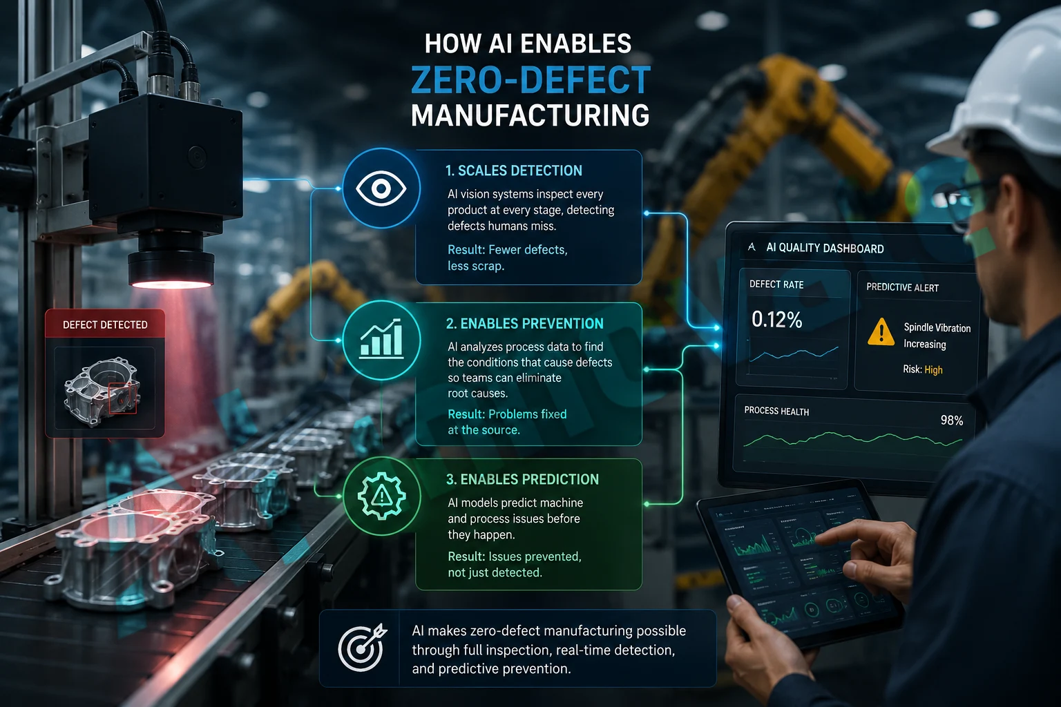
AI is what makes zero defect manufacturing practical, because it enables full inspection, real-time detection, and predictive prevention at production speed. Earlier quality methods couldn’t inspect every part or predict failures, so getting near zero was out of reach. AI changes that in three ways.

  • First, it scales detection. Computer vision systems using deep learning can inspect every product at every stage, not just a sample, catching defects human inspectors miss and reducing scrap. Strong defect detection in manufacturing is the foundation everything else builds on.
  • Second, it enables prevention. By analyzing process data, AI identifies the conditions that lead to defects so teams can eliminate root causes, which is the core of AI-driven quality control.
  • Third, it enables prediction. AI models forecast machine and process issues before they happen, supporting the predict-and-prevent strategy that gets closest to zero. On the lines we work with, it’s this predictive layer that separates a real zero-defect program from one that’s just inspecting harder.
How Does AI Enable Zero-Defect Manufacturing

The Benefits Show Up Long Before You Reach Zero

The benefits show up well before you ever reach zero, which is what makes the pursuit worthwhile.

Lower scrap and rework come first, since preventing defects costs far less than fixing or discarding finished products. Fewer escapes mean fewer recalls, warranty claims, and the reputation damage that follows a quality failure in the field. Over time, the cost of quality drops as spending shifts from correcting problems to preventing them. And because zero defect quality control generates data at every step, AI for quality assurance gives manufacturers the visibility to keep improving rather than firefighting. Even partial progress toward zero pays for itself.

What Challenges Stand in the Way?

The main challenges are cost, data, complexity, and diminishing returns. None of them is a reason to avoid the goal, but each is worth understanding before committing.

  • Cost and complexity. Full inspection and predictive systems require investment in cameras, sensors, edge hardware, and integration.
  • Data requirements. Predictive prevention depends on quality historical data, which many plants find fragmented or incomplete.
  • Diminishing returns. As you approach zero, each further gain costs more, so there’s a practical point where the effort outweighs the benefit for some operations.
  • Process variation. Highly variable materials or low-volume, high-mix production make patterns harder to learn and defects harder to predict.

The honest takeaway is that zero defect manufacturing is a journey of continuous improvement, not a switch you flip.

How AI-innovate Supports Zero-Defect Manufacturing

We help manufacturers move toward zero defects by combining full inspection, root-cause prevention, and predictive capability on systems tuned to their actual production. Getting close to zero isn’t about inspecting harder; it’s about moving quality upstream, and that’s what we focus on.

The components we deploy:

  • AIxEye delivers real-time defect detection and process optimization, inspecting every product at production speed rather than relying on samples.
  • AIxCore is the industrial AI edge computer powered by NVIDIA Jetson Orin AGX, running inference on-site so detection and prevention happen fast enough to act on.
  • AIxCam provides simulation tools and synthetic data generation, helping you train models on rare defects that haven’t appeared often enough on the line to learn from.
  • AIxAM detects surface and geometry defects on three-dimensional parts using multi-view images and depth data, widening the range of defects you can catch and prevent.

Wherever you are on the path toward zero defects, the foundation’s the same: full visual data, explainable AI, and systems built for real production. Book a demo and we’ll talk through where your biggest quality gains are. Reach us at Info@ai-innovate.com or +1 (514) 813-1809.

How AI-innovate Supports Zero-Defect Manufacturing

Final Thoughts

Zero-defect manufacturing isn’t a promise that nothing will ever go wrong. It’s a commitment to eliminating defect causes instead of accepting them, and to moving quality further upstream over time. Understood that way, the goal stops being a slogan and becomes a practical direction that pays off long before you reach perfection.

AI is what’s made that direction realistic. By enabling full inspection, root-cause prevention, and defect prediction at production speed, it closes the gap older methods never could. No system hits a literal zero, but the manufacturers chasing it, with the right technology behind them, end up with less waste, fewer escapes, and a real edge on quality.

Frequently Asked Questions

Is zero-defect manufacturing actually realistic?

Not literally. No system reaches 100 percent perfection, but zero-defect manufacturing is a target that drives teams to eliminate defect causes rather than accept them. The pursuit gets you far closer to zero than treating some failure as normal.

The idea grew out of the twentieth-century quality movement and was formalized alongside Six Sigma in the 1980s, popularized by companies like Motorola and General Electric. Modern zero-defect manufacturing is its Industry 4.0 evolution.

Six Sigma is a statistical methodology for reducing variation to a defined defect rate. Zero-defect manufacturing is a broader philosophy aimed at eliminating defects entirely. They overlap, and many ZDM programs use Six Sigma tools.

AI can’t guarantee zero, but it gets manufacturers far closer than older methods by enabling full inspection, root-cause prevention, and defect prediction. It’s the enabler that makes meaningful progress toward the goal realistic.

Common measures include defects per million opportunities, scrap and rework rates, escape rates, and cost of quality. The trend over time matters more than any single number.

Often yes, if the cost of defects is high. The technology scales down to single lines, and even partial progress toward zero reduces scrap and protects customer trust. The question is whether your defect costs justify the investment.

No. It builds on existing inspection, adding full coverage and predictive prevention on top of the checks you already run. The aim is moving quality upstream, not tearing out what works.

Ai-Innovate uses only high-quality sources, including peer-reviewed studies, to support the facts within our articles.

  1. Zero-Defect Manufacturing for Engineers. Tencom (2026). Covers the definition of ZDM, its roots in twentieth-century quality philosophies, and its formalization alongside Six Sigma in the 1980s. https://www.tencom.com/blog/zero-defect-manufacturing-for-engineers
  2. Zero Defect Manufacturing in the Era of Industry 4.0. Frontiers (2021). Describes how ZDM incorporates AI, ML, and big industrial data into quality control loops to predict and prevent defects at product and process levels. https://www.frontiersin.org/research-topics/27428/zero-defect-manufacturing-in-the-era-of-industry-40-for-achieving-sustainable-and-resilient-manufacturing
  3. Role of Industry 4.0 in Zero-Defect Manufacturing: A Systematic Literature Review. ScienceDirect (2024). Defines the four core ZDM strategies: detection, repair, prediction, and prevention. https://www.sciencedirect.com/science/article/pii/S221384632400289X
  4. Zero-Defect Manufacturing: The Approach for Higher Manufacturing Sustainability in the Era of Industry 4.0. Taylor & Francis (2021). Explains the Detect-Repair, Detect-Prevent, and Predict-Prevent approaches. https://www.tandfonline.com/doi/full/10.1080/00207543.2021.1987551
  5. Artificial Intelligence for Quality Defects in the Automotive Industry: A Systematic Review. PMC / NIH (2025). Documents how AI and CNN-based computer vision strengthen defect detection, reduce scrap, and enable proactive maintenance in zero-defect strategies. https://www.ncbi.nlm.nih.gov/pmc/articles/PMC11902312/
  6. Zero Defect Manufacturing. ATRIA Innovation (2024). Covers the use of computer vision and deep learning to detect defects at every stage of production. https://atriainnovation.com/en/blog/zero-defect-manufacturing/
Glass Defect Detection Using AI

AI-Powered Glass Defect Detection: How Automated Inspection Improves Quality Control

A scratch invisible to the naked eye can shatter a windshield under stress. Glass is everywhere in high-stakes manufacturing, yet it remains one of the hardest materials to inspect reliably. Its transparency, reflectivity, and sensitivity to lighting angle mean that the same defect can appear obvious from one position and invisible from another, which is why glass quality control has historically depended on slow, subjective manual checks.

This guide covers what glass defect detection actually involves, the specific flaws that matter most, why glass is uniquely difficult to inspect, how AI changes the equation, and where it delivers the most value.

What Is Glass Defect Detection?

Glass defect detection is the process of identifying surface, internal, and structural flaws in glass products before they reach downstream assembly or the end customer. It applies across flat glass sheets, bottles and containers, automotive glazing, display panels, lenses, and specialty optics.

The core challenge is that glass behaves optically in ways most materials don’t. It transmits, reflects, and refracts light simultaneously, which means cameras and human eyes alike can struggle to separate a real defect from a normal optical effect. That’s what makes glass inspection a distinct problem.

What Are the Most Common Glass Defects?

The most common glass defects fall into three categories: surface defects, internal defects, and structural defects. Each has different causes, different visual signatures, and different consequences if missed.

Surface Scratches and Chips

Scratches are the most frequent glass defect, caused by mechanical contact or friction during handling, transport, or processing. Shallow scratches can be nearly invisible under standard lighting, which makes them easy to miss manually. Chips and shells typically appear on edges from impact during handling and are easier to spot but critical to reject.

Internal Bubbles and Inclusions

Bubbles (also called seeds) and inclusions are foreign particles or gas pockets trapped inside the glass during melting. They originate from batch impurities or furnace wear. These defects reduce glass strength and, in tempered glass, can cause spontaneous breakage, which is why they’re treated as serious safety risks in automotive and architectural applications.

Coating Defects and Pinholes

Coated glass products (low-E architectural glass, anti-reflective lenses, display panels) can develop voids, pinholes, or uneven coverage during the coating process. These appear as tiny exposed spots that compromise performance and are especially hard to detect on transparent substrates.

Cracks and Stress Fractures

Cracks can form during thermal processing, handling, or from internal stress concentrations. In container glass, split-finish cracks are nearly invisible but compromise the seal integrity of the bottle or jar.

Contamination

Dust, grease, water spots, and other contaminants can become embedded or trapped in the glass structure. They’re cosmetically unacceptable in most applications and can interfere with downstream coating or bonding processes.

Heat-Treating Defects

Improper tempering or cooling can cause bows, ripples, or warping across the glass surface. These structural defects affect both performance and appearance and are distinct from surface flaws because they involve the geometry of the piece itself.

What Are the Most Common Glass Defects

Why Is Glass Inspection Harder Than Other Materials?

Glass inspection is harder because the material’s transparency and reflectivity create optical effects that confuse both human inspectors and traditional machine vision systems. On an opaque material like metal or wood, machine vision for defect detection sees surface features directly. On glass, it sees through the surface, reflects off it, and refracts through it, all at once.

The specific challenges include:

  • Transparency means defects and background blend together, making contrast-based detection unreliable.
  • Reflectivity creates glints, highlights, and mirror effects that can look like defects or mask real ones.
  • Angle dependency means the same scratch can be visible at one lighting angle and invisible at another.
  • Variable glass types (tempered, laminated, curved, coated) each behave differently under the same lighting.
  • Subtle defects like shallow scratches, micro-bubbles, and coating pinholes sit at or below the threshold of what rule-based vision reliably catches.

Manual inspection adds its own problems on top of these. Fatigue, subjectivity, and slow throughput make it nearly impossible to scale for high-volume glass production. An experienced inspector might catch most defects in a small batch, but consistency drops sharply over a full shift of looking through transparent material under changing light.

What Methods Does AI Use to Detect Glass Defects?

AI detects glass defects by training deep learning models to recognize flaws across multiple lighting conditions and glass types, learning to separate real defects from the optical noise that confuses rule-based systems.

The most common approaches in industrial glass inspection are:

  • Convolutional neural networks (CNNs) such as ResNet, EfficientNet, and MobileNet for defect classification, identifying whether a region contains a scratch, bubble, inclusion, or other flaw.
  • Object detection models like YOLO variants and Faster R-CNN for locating and classifying defects simultaneously, drawing bounding boxes around each flaw with a defect-type label.
  • Instance segmentation models like Mask R-CNN for pixel-level defect mapping, which is especially useful for scratches on transparent surfaces where the defect boundary matters.
  • Synthetic data generation using diffusion models to create artificial defect images when real defective samples are scarce, addressing the class imbalance problem that plagues glass inspection datasets.

These are the core architectures behind modern AI for material defect identification, and each one trades off speed against precision depending on what the line needs.

Recent research using improved ResNet-50 architectures has achieved 97.2% detection accuracy for glass defects with a false detection rate below 0.5%, processing at 25 frames per second at production-line edge speed.

This performance holds across multiple glass types and defect categories, from flat float glass to curved automotive panes. The consistency of these results across recent research (2021-2025) demonstrates that AI has reached a reliable threshold where accuracy and speed both exceed what manual inspection can sustain over a full production shift.

On the lines we work with, the practical difference is that AI holds its accuracy across lighting variation, glass curvature, and shift changes, all the conditions where manual and rule-based inspection break down.

Where Are Glass Defects Most Critical?

Glass defects are most critical in industries where a missed flaw creates a safety risk, a regulatory violation, or a high-cost field failure. Four industries stand out.

Automotive Glass

Windshields, side windows, mirrors, and lighting covers all require defect-free glass. An inclusion or stress fracture in a windshield is a direct safety hazard. Automotive glass inspection demands high-speed inline detection with zero tolerance for critical defects like inclusions and cracks.

Pharmaceutical Packaging

Glass vials, bottles, ampoules, and syringes must be free of cracks, chips, and particulate contamination. A defect that compromises the seal or introduces contamination into a drug product can trigger a recall. Pharma glass inspection operates under strict regulatory standards where traceability and documentation matter as much as detection itself.

Electronics and Displays

Smartphone screens, tablet panels, camera lenses, and optical components all require flawless glass surfaces. Even a micro-scratch on a display cover glass is a reject. The combination of high volume, small defect size, and tight tolerances makes this one of the most demanding glass inspection applications.

Architectural and Construction Glass

Float glass, tempered panels, and coated architectural glass are inspected for scratches, coating defects, and heat-treating distortion. Tolerances are generally wider than automotive or electronics, but the sheer size of the panels (often several meters) makes full-surface coverage a throughput challenge that manual inspection can’t scale for.

Where Are Glass Defects Most Critical

What Changes When You Switch to AI Glass Inspection?

The biggest change is consistency. AI removes the angle dependency, fatigue, and subjectivity that limit manual and rule-based inspection on glass.


Factor Manual Inspection Traditional Machine Vision AI-Based Inspection
🔍 Handles Transparency & Reflections Partially, depends on inspector skill Poorly, prone to false calls Well, learns to filter optical noise
🎯 Defect Consistency Varies by operator and shift Consistent but rigid Consistent and adaptive
⚡ Throughput Slow, limits line speed Fast but limited by rules Fast and flexible
🔬 Subtle Defect Detection Unreliable at speed Misses low-contrast flaws Catches micro-defects reliably
🔄 Adaptability to New Products Immediate but subjective Requires reprogramming Requires retraining with new data
📊 Data & Traceability Manual documentation Basic logging Automatic classification, logging, and trend analysis

Beyond consistency, AI inspection gives glass manufacturers something manual checks can’t: data. Every defect is classified by type, size, and location automatically, which feeds into trend analysis, process control, and quality audits. That visibility is what turns inspection from a pass/fail gate into a tool for continuous improvement, the kind of real-time surface defect detection that drives yield gains over time.

How AI-innovate Supports Glass Defect Detection

We help glass manufacturers deploy AI inspection systems built around their specific glass types, defects, and production requirements, not generic datasets.

  • AIxEye performs real-time defect detection on the line, identifying scratches, chips, bubbles, inclusions, coating defects, contamination, and cracks across flat glass, automotive glazing, pharmaceutical containers, and display panels.
  • AIxCore is our NVIDIA Jetson Orin AGX-powered edge AI computer, delivering low-latency inspection and real-time processing directly on-site.
  • AIxCam provides camera simulation and synthetic data generation, helping train models for rare defects such as inclusions, stress fractures, and coating failures.
  • AIxAM analyzes multi-view images and depth data to detect surface and geometry defects on curved glass, containers, and other 3D glass products.


Every deployment starts with your glass type, defect profile, line speed, and quality requirements. From there, we design the inspection system around your production environment.

Book a demo and we’ll scope a glass inspection solution tailored to your products, defects, and throughput goals. Reach us at Info@ai-innovate.com or +1 (514) 813-1809.

Final Thoughts

Glass earns its reputation as one of the hardest materials to inspect. Transparency, reflectivity, and angle-dependent visibility make it a problem that manual checks and rule-based vision both struggle to solve consistently. AI changes the equation by learning to see through the optical noise, holding accuracy across shifts, and catching the subtle flaws that drive the costliest escapes.

The manufacturers getting the best results pair AI with the right lighting, cameras, and data pipeline for their specific glass type. They treat the model as part of a workflow, not a finished product on day one, and they use the inspection data to improve their process, not just reject bad parts.

Frequently Asked Questions

Can AI detect defects inside glass, not just on the surface?

AI can detect internal defects like bubbles and inclusions when the imaging setup is designed for it, typically using backlighting or transmitted light to make internal flaws visible. Surface-only lighting will miss subsurface defects regardless of how good the AI model is.

AI models trained on glass learn to distinguish between optical artifacts (glints, refractions, transparency effects) and real defects. This is one of the main advantages over rule-based vision, which tends to either over-flag reflections as defects or miss real flaws hidden behind them.

Usually yes. A model trained on flat float glass will underperform on curved automotive glass or coated display panels because the optical behavior changes. Retraining on the new glass type is far less work than building a model from scratch, but it’s a step that shouldn’t be skipped.

Modern object detection models run fast enough for inline inspection at full production speed. The exact throughput depends on resolution, camera setup, and glass size, but deep learning models routinely process frames in milliseconds, which keeps up with high-speed glass lines.

Data scarcity for rare defects. Common flaws like scratches are easy to collect, but critical defects like inclusions or stress fractures are rare by nature. Synthetic data generation helps close this gap by creating artificial training examples of uncommon defects.

Yes, if the model is trained with that distinction. A well-labeled dataset that separates cosmetic-only flaws (light surface marks) from structural risks (inclusions, cracks) lets the model classify severity, not just presence, which supports smarter accept/reject decisions.

No. The technology scales down to single-line deployments. The key factor isn’t production volume but whether your defect cost and quality requirements justify the investment, which is often the case even for smaller operations producing safety-critical or high-value glass products.

Ai-Innovate uses only high-quality sources, including peer-reviewed studies, to support the facts within our articles.

  1. Research on the Application of Computer Vision and Deep Learning in Green Building Material Quality Inspection. Proceedings of the 2025 International Conference on Artificial Intelligence and Smart Manufacturing. Demonstrates improved ResNet-50 architecture achieving 97.2% detection accuracy on glass defects with false detection rate below 0.5% at 25 fps edge processing speed on a 120,000-image dataset. https://dl.acm.org/doi/10.1145/3756423.3756435
  2. Enhancing Glass Defect Detection with Diffusion Models: Addressing Imbalanced Datasets in Manufacturing Quality Control. arXiv (2025). Addresses class imbalance in glass defect datasets and proposes Denoising Diffusion Probabilistic Models (DDPMs) for synthetic data generation of rare defects. https://arxiv.org/pdf/2505.03134
  3. A lightweight and robust detection network for diverse glass surface defects via scale- and shape-aware feature extraction. Engineering Applications of Artificial Intelligence (2026). Comprehensive review of recent glass defect detection methods (2022-2024), noting advances in attention mechanisms and multi-scale feature extraction for handling variable defect sizes and shapes. https://www.sciencedirect.com/science/article/abs/pii/S0952197625006402
  4. Optimizing Defect Detection on Glossy and Curved Surfaces Using Deep Learning and Advanced Imaging Systems. Sensors (2025). Addresses defect detection on reflective and curved glass surfaces using ResNet-50 and VGG-16 architectures, directly tackling the transparency and reflectivity challenges. https://www.ncbi.nlm.nih.gov/pmc/articles/PMC12031545/
  5. Context-Enhanced Network with Spatial-Aware Graph for Smartphone Screen Defect Detection. Sensors (2024). Demonstrates deep learning methods for detecting defects in high-precision glass screens using attention mechanisms and graph reasoning. https://www.ncbi.nlm.nih.gov/pmc/articles/PMC11175082/
  6. Cognex. Glass Inspection: AI-Powered Glass Quality Control. Industry reference on the challenges of transparency, reflectivity, and variable lighting in glass inspection, and how AI addresses them. https://www.cognex.com/en/applications/automated-defect-detection/material-quality-inspection/glass-defect-detection
  7. Sari, F. (2022). Deep Learning Application in Detecting Glass Defects with Color Space Conversion and Adaptive Histogram Equalization. International Information and Engineering Technology Association. Demonstrates YOLO-V3 achieving above 97% precision/recall on glass jar scratch and bubble defects with color-space preprocessing methods. https://www.iieta.org/download/file/fid/73685
  8. Image-based surface scratch detection on architectural glass panels using deep learning approach (2021). ScienceDirect. Demonstrates Mask R-CNN achieving 96.5% mAP for pixel-level scratch detection on transparent glass surfaces. https://www.sciencedirect.com/science/article/abs/pii/S0950061821004773
wood defect detection using ai

Wood Defect Detection Using AI for Smarter Quality Control

A finished oak panel can be worth ten times what the same board was as rough lumber. A missed crack or a misjudged knot can wipe that value out in a single cut. Wood is unforgiving that way: it carries enormous variability, the line between a feature and a flaw is hard to see, and every grading decision ripples through downstream yield, cost, and customer trust. That’s why wood defect detection has stayed labor-intensive long after other industries automated their inspection.
This guide covers the defects that drive most rejects on a wood line, how they’re being caught today, where AI is changing the economics of wood surface inspection, and what to look for if you’re ready to move past manual grading.

Transform Wood Inspection with AI-Powered Defect Detection

Move beyond manual grading and rule-based machine vision. Learn how machine vision for defect detection and deep learning improve accuracy, speed, and consistency in industrial wood inspection systems.

What Is Wood Defect Detection?

Wood defect detection is the process of identifying flaws on wood surfaces, such as knots, cracks, and resin pockets, before the piece moves further down the production line. It applies across sawmills, plywood and panel production, flooring, furniture manufacturing, and structural lumber, anywhere the surface quality of wood determines the value of the finished product.
The challenge with wood, more than with most materials, is that natural features and real defects can look very similar. A live knot might be acceptable in one product and rejectable in another. Grain variation is normal but can be mistaken for a flaw. Getting the call right consistently is what separates good wood inspection from a steady stream of false rejects and customer escapes.

What Is Wood Defect Detection

What Are the Most Common Wood Surface Defects?

The most common wood surface defects are knots, cracks, resin pockets, wormholes, and discoloration. Public industrial datasets used to train modern detection models typically label ten or more distinct defect classes, but most production lines focus on the handful that drive the majority of rejects.

Live and Dead Knots

A live knot is firmly attached to surrounding wood and sometimes cosmetically acceptable, while a dead knot is loose or detached from the wood around it. Dead knots are usually the higher-priority defect because they can fall out and create holes, but both need to be located accurately to decide whether to cut around them.

Resin Pockets and Pitch

Resin pockets are cavities filled with sap or pitch. They affect appearance and can interfere with finishing and gluing, which makes them a recurring issue in furniture and flooring lines.

Wormholes and Insect Damage

Wormholes are small voids left by insect activity. They’re cosmetic in low-grade products but reject-grade in higher-value finishes, so accurate classification matters more than detection alone.

Discoloration and Stain

Blue stain, mineral streaks, and other discoloration usually don’t affect strength but reduce visual grade in finish-critical applications. They’re some of the hardest defects to call reliably because they shade gradually into normal grain variation.

Missing Knots, Marrow, and Quartzity

These are less common but show up in detailed defect taxonomies. Missing knots are holes where a knot has fallen out, marrow refers to pith at the center of the tree, and quartzity describes mineral-rich abnormalities. They’re worth knowing about if you’re building a model that needs to handle the full range a real sawmill produces.

How Is Wood Surface Inspection Done in 2026?

Wood surface inspection is done through a combination of manual visual checks, traditional machine vision systems, and increasingly, AI-based vision systems trained on wood-specific defect data. Each approach handles different parts of the problem.

Approach Best At Limitation
Manual Visual Inspection Subjective judgment on wood grade and finish quality Slow, inconsistent across shifts, fatigue-prone
Traditional Machine Vision High-speed detection of clear, consistent defects Struggles with natural variation and subtle wood defects
AI / Deep Learning Vision Detecting subtle and irregular defects across varied grain patterns Requires quality training data and ongoing model tuning

Most production lines today still rely on human inspectors for final grading, with traditional vision handling speed-critical checks. The shift toward AI is driven by the same problem that’s hard for both: telling a real defect apart from a natural feature when the two look almost identical.

How Does AI Improve Wood Defect Detection?

AI improves wood defect detection by learning to distinguish defects from natural grain variation, something rule-based vision systems struggle with on a material as varied as wood. Convolutional neural networks (CNNs) and modern object detection models like YOLO can be trained on thousands of annotated wood defect images and then classify defects in real time as boards move down the line.

Published research shows real performance on real wood lines. Deep learning approaches have reached defect classification accuracy above 99% on solid wood panels, with detection times near one second per piece including preprocessing. Single-stage object detection models such as YOLO variants and two-stage models like Faster R-CNN both perform strongly across knots, cracks, and resin defects, with the choice between them depending on the speed and accuracy tradeoff a specific line needs.

The practical advantages on a wood line look like this:

AI-Powered Wood Inspection vs Traditional Inspectio

This is one of the strongest cases for AI for material defect identification, because the underlying problem (high natural variation plus rare-but-serious defects) is exactly what learning-based methods are built to solve.

Where Does AI Fit on a Wood Production Line?

AI fits best as the inspection layer between raw scanning and downstream cutting or grading decisions. Cameras capture each board, the AI model classifies and locates defects, and the line uses that data to decide what happens next.
A typical setup looks like this:

1
📷

Industrial Cameras

Capture high-resolution images of every board under controlled lighting conditions.

➜
➜
3
✂️

Decision Logic

Uses defect type and location to determine trimming, cutting, grading, downgrade, or rejection actions.

➜
4
📈

Continuous Learning

Flagged samples improve future model performance, detection accuracy, and overall inspection consistency.

Defects that go beyond surface flaws, such as hidden voids or internal density variations, may still need X-ray inspection. But for everything visible on the surface, an AI vision system delivers far higher throughput and consistency than manual grading.

What Are the Challenges of AI-Based Wood Inspection?

The main challenges are training data quality, separating defects from acceptable variation, and adapting to different wood species. Wood is highly variable, and a model trained on one species or grade can underperform on another without retraining.

Specific issues to plan for:

  • Annotated training data needs to cover the species, grade, and defect mix your line actually produces.
  • Lighting consistency matters more than usual on wood because grain and color can dramatically change appearance.
  • Class imbalance is common: live knots are everywhere, marrow and missing knots are rare. Models need careful handling so rare defects aren’t missed.
  • Threshold tuning decides whether borderline cases (a small live knot, light discoloration) are flagged or passed.


These are solvable with the right data pipeline and tuning process, but they’re worth knowing about before committing to a system. The strongest results come from surface defect detection setups that treat the model as part of a workflow, not as a finished product on day one.

How AI-innovate Supports Wood Surface Inspection

We help wood manufacturers bring AI inspection onto the line in a way that matches their real material, not a generic demo. The goal is reliable defect calls on your actual wood, at your actual line speed.

At AI-innovate, we support wood defect detection with:

  • AIxEye for real-time defect detection and process optimization, identifying knots, cracks, resin pockets, discoloration, and other surface flaws across wood production lines
  • AIxCore, an industrial AI edge computer powered by NVIDIA Jetson Orin AGX, delivering real-time image processing and reliable on-site machine vision for inspection workflows
  • AIxCam, advanced simulation tools for camera testing and synthetic data generation, helping you build out training datasets for rare defects like missing knots or marrow that are hard to capture in volume
  • AIxAM, which detects surface and geometry defects on 3D objects, including cracks, deformation, and assembly misalignment, by analyzing multi-view images and depth data in real time


Whether you’re upgrading inspection on a single panel line or scaling wood quality control across multiple facilities, the foundation is the same: reliable visual data, explainable AI, and industrial-grade deployment. Book a demo and we’ll help you scope it around your species, defects, and throughput.

Final Thoughts

Wood is one of the harder materials to inspect well, because the same features that give it value, grain, color, and natural character, are also what make defects hard to call consistently. The strongest setups don’t try to remove that variability. They use AI to learn it, so the system can separate a live knot from a dead one and a real crack from harmless grain.
Pair that with high-speed cameras, good lighting, and a feedback loop, and inspection becomes a reliable part of the line rather than a bottleneck. Manufacturers who get this right see fewer escapes, more usable yield from each board, and steadier grading across every shift.

Ai-Innovate uses only high-quality sources, including peer-reviewed studies, to support the facts within our articles.

  1. Shah, H., Saarela, E., Korkeakangas, T., & Pitkäaho, T. (2026). A comprehensive review of automatic defect detection in wooden surface inspection. Applied Computing and Intelligence. Review of single-stage and two-stage deep learning models for wood defect detection and the move beyond manual and X-ray methods. https://www.aimspress.com/article/doi/10.3934/aci.2026001
  2. Detecting Defects on Solid Wood Panels Based on an Improved SSD Algorithm. PMC / NIH. Sets out the production-line accuracy and speed requirements (above 95% on live knots, dead knots, and cracks at 50 m/min). https://www.ncbi.nlm.nih.gov/pmc/articles/PMC7570981/
  3. FDD-YOLO: A Novel Detection Model for Detecting Surface Defects in Wood. MDPI Forests (2025). Defines the multi-class wood defect taxonomy used in modern detection datasets, including live knot, dead knot, knot-with-crack, knot-missing, crack, marrow, and resin. https://doi.org/10.3390/f16020308
  4. Bilateral Defect Cutting Strategy for Sawn Timber Based on Artificial Intelligence Defect Detection Model. PMC / NIH. Demonstrates a YOLO-based framework for locating and classifying live knots, dead knots, cracks, and insect holes in sawn timber. https://pmc.ncbi.nlm.nih.gov/articles/PMC11510799/
  5. Zenodo (2021). Supporting data for deep learning and machine vision based approaches for automated wood defect detection. Open dataset with over 43,000 labeled wood surface defects across ten classes. https://zenodo.org/record/4694695.

Frequently Asked Questions About AI Wood Defect Detection

Common questions manufacturers ask when evaluating AI-powered wood inspection systems and machine vision technology.

Yes. Trained on labeled wood images, AI models can classify a knot as live, dead, knot-with-crack, or missing and determine whether it should be treated as a defect according to your grading rules. This type of judgment is one of the key advantages AI has over traditional rule-based vision systems.

Usually yes, at least partially. A model trained primarily on pine may not perform as accurately on oak, maple, or beech because grain patterns, color, and defect appearance vary significantly between species. Retraining with species-specific data is typically much faster than building a model from scratch.

Modern AI inspection systems are designed for industrial production environments. Research demonstrates defect classification in approximately one second per panel, while advanced object detection models can operate at conveyor speeds exceeding 50 meters per minute.

The required dataset size depends on the variety of defects and natural grain variations present in your production line. Public datasets containing 20,000 to 40,000 labeled wood defect images provide a useful starting point, but the highest-performing models are typically trained with examples collected directly from the target manufacturing environment.

Not from surface images alone. AI vision systems excel at identifying visible defects such as knots, cracks, resin pockets, and discoloration. Detecting internal defects like hidden voids, density variations, or internal cracks generally requires technologies such as X-ray or ultrasound inspection, often combined with AI-based classification.

Wood exhibits significant natural variation in grain, color, and texture. Traditional machine vision relies on predefined rules that can struggle with this variability. AI learns from real examples and can distinguish between acceptable wood characteristics and genuine defects, reducing both false rejects and missed defects.

Costs vary based on line speed, camera requirements, lighting configuration, integration complexity, and AI model deployment. Most manufacturers justify the investment through reduced manual grading labor, lower scrap rates, improved quality consistency, and better downstream product value.

AI-Powered Weld Defect Detection

AI-Powered Weld Defect Detection : A 2026 Complete Guide

A bad weld hardly goes unnoticed. It turns into rework, delays, failed inspections, or problems that show up later when the part is already in service. In an industrial environment, that’s a serious risk since welding lines move fast and even small defects can repeat across hundreds of parts before anyone catches them. While manual inspection is still important, the reality is that it’s getting harder to maintain consistent checks as production speeds increase. To help the inspectors on the floor, many manufacturers have turned to AI weld defect detection.
In this article, we inspect the effects of AI on weld defect detection, the type of defects AI can catch, how it compares to traditional inspection, and where the ROI is particularly noticeable.

Improve Weld Quality with Real-Time AI Inspection

Detect weld defects instantly with advanced computer vision and AI. Increase inspection consistency, reduce manual errors, and ensure every weld meets quality standards.

How AI Improves Real-Time Weld Defect Detection

The biggest advantage of automated weld inspection is timing.
The earlier a defect gets caught, the cheaper it is to deal with. Once a bad weld moves downstream into machining, painting, assembly, or shipping, the cost of fixing it climbs quickly. Most manufacturers have learned that lesson the expensive way at some point.

Instead of relying only on end-of-line checks, newer systems monitor weld seams while welding is actually happening. Cameras track the weld visually, thermal sensors watch heat behavior, and acoustic systems listen for changes in the welding process that don’t sound right.

Most automated weld quality control systems focus on:

  • continuous weld seam inspection
  • real-time defect alerts
  • process consistency
  • defect classification
  • traceability for audits and compliance

How Thermal AI Detects Welding Defects

Every weld creates a thermal pattern. When the weld process becomes unstable, that pattern changes too.
Thermal inspection systems use infrared imaging to track how heat moves through the weld during and after welding. AI models learn what a healthy weld profile looks like and flag the ones that drift outside normal behavior.

This works especially well for defects connected to heat inconsistency, including:

  • incomplete fusion
  • poor penetration
  • overheating
  • unstable cooling
  • potential internal defects

On robotic welding lines, this becomes useful very quickly. If a welding parameter drifts slightly out of spec, defects can repeat across large batches before operators notice anything visually.
We’ve seen this matter most in automotive and pipeline manufacturing, where a small process issue can affect thousands of welds before final inspection catches it.

How Machine Vision AI Improves Weld Seam Inspection

Industrial cameras capture images of the weld seam while software analyzes bead shape, edge consistency, contour depth, texture variation, and surface abnormalities.
The system compares those patterns against trained defect examples instead of relying entirely on rigid pass/fail rules. Instead of looking for one perfect-looking weld, the system learns the difference between normal variation and actual defects.
However, false-call fatigue can become a real issue on production floors. If operators spend all day clearing unnecessary inspection alerts, trust in the system disappears pretty quickly.

Machine vision weld inspection is commonly used for:

  • robotic welding cells
  • automotive structural welding
  • pressure vessel manufacturing
  • heavy fabrication
  • structural steel production

This Topic might also interest you :

How Acoustic Emission AI Identifies Hidden Weld Defects

Not every weld problem shows up clearly on the surface, and that’s where acoustic monitoring is applied.
During welding, the arc, cooling process, and material interaction all create sound patterns. When something changes, instability, cracking, inconsistent penetration, the sound changes too.

Acoustic emission systems help identify welding conditions associated with:

  • unstable weld pools
  • arc interruptions
  • lack of penetration
  • process inconsistency
  • potential internal cracking

On its own, acoustic monitoring usually isn’t enough to run a full inspection process. But when it’s layered together with machine vision and thermal monitoring, it gives manufacturers another way to catch defects that optical systems might miss.

The strongest inspection systems usually combine multiple inspection methods instead of relying on only one.

What Welding Defects Can AI Detect?

The exact defects matter because each one creates different structural risks and different downstream problems. Most weld defects fall into a handful of major categories.

Porosity and Gas Pocket Detection

Porosity happens when gas gets trapped inside the weld, leaving cavities behind.
A little porosity might not matter much depending on the application. Too much of it weakens the weld and reduces long-term durability. The challenge is that porosity doesn’t always look obvious from the surface.
Inspection systems usually detect it through:

  • texture irregularities
  • seam inconsistencies
  • thermal cooling variation

This matters most in industries where welds face repeated stress over time, especially aerospace, automotive, and pipeline manufacturing.

Crack Detection in Welded Joints

Cracks are one of the highest-risk weld defects because they tend to spread instead of staying contained.
Inspection systems may need to identify:

  • longitudinal cracks
  • transverse cracks
  • crater cracks
  • heat-affected zone cracking

Some cracks are easy to spot. Others are microscopic and only become visible under the right lighting or thermal conditions. This is one of the areas where automated inspection often performs better than manual inspection in high-throughput environments.

Incomplete Fusion and Penetration Detection

Incomplete fusion means the weld never bonded properly to the base material, and incomplete penetration means the weld didn’t fully extend through the joint.
Both defects weaken the structure significantly. The problem is that these defects are often difficult to confirm visually, especially on fast-moving production lines.
Thermal monitoring helps because inconsistent penetration changes the weld’s heat profile. Machine vision systems also identify seam irregularities connected to poor bonding conditions.

Weld Spatter and Surface Contamination Detection

Spatter isn’t always structurally dangerous, but it creates problems quickly in high-precision manufacturing environments.
Excessive spatter can affect:

  • coating adhesion
  • robotic fit-up
  • downstream assembly
  • cosmetic quality
  • sensor positioning

Inspection systems also look for oxidation marks, contamination residue, and inconsistent bead shape. This matters most in industries where appearance and structural quality both matter, particularly automotive and aerospace manufacturing.

This Topic might also interest you :

Undercut and Overlap Detection

Undercut happens when excess heat removes material along the weld edge, creating a groove that weakens the joint. Overlap is the opposite problem: weld material spills beyond the joint without bonding correctly underneath.
Both defects usually point to unstable welding parameters. Machine vision systems identify them by analyzing:

  • contour depth
  • seam continuity
  • edge geometry
  • bead consistency

One advantage of automated inspection here is consistency. The system checks every weld the same way, whether it’s the first weld of the day or the ten-thousandth.

Manual vs AI Weld Inspection Systems

Experienced inspectors are often better at handling unusual edge cases or defects that don’t follow predictable patterns. But repetitive inspection at production speed is where automated systems start pulling ahead.

Inspection Method Consistency Real-Time Detection Fatigue Impact Scalability
Manual Inspection Variable Limited High Limited
Traditional Vision Systems Moderate Partial None Moderate
AI Weld Inspection High Yes None High

Comparison of manual, traditional, and AI-powered weld inspection methods across consistency, real-time detection, operator fatigue, and scalability.

The more repetitive the inspection becomes, the harder it gets to maintain consistency manually. Although, that doesn’t mean manufacturers are removing people from inspection completely.

Most strong inspection setups split the work like this:

  • automated systems handle continuous inspection
  • software handles classification and anomaly detection
  • operators review uncertain or high-risk calls

That’s the same hybrid model becoming common across manufacturing quality control more broadly.

Where Automated Weld Inspection Delivers the Highest ROI

Not every welding environment benefits equally from automation. The strongest ROI usually appears where throughput, defect risk, and inspection volume all collide.

Automotive Weld Inspection

Automotive manufacturing is one of the clearest use cases for automated weld inspection.
Modern vehicle production involves thousands of welds moving through robotic cells at high speed. If a welding parameter drifts slightly out of spec, defects can repeat across huge production batches before manual inspection catches the problem.

Manufacturers use automated weld inspection to improve:

  • chassis weld consistency
  • EV battery enclosure quality
  • robotic welding traceability
  • throughput stability
  • warranty reduction

Pressure Vessel and Pipeline Weld Inspection

Pressure vessel and pipeline welds carry much higher structural risk than most manufacturing welds.

Failures here can mean:

  • shutdowns
  • environmental damage
  • compliance failures
  • expensive repairs
  • serious safety incidents

That’s why inspection standards are stricter and defect tolerance is lower.
Thermal monitoring and acoustic analysis become especially useful in these environments because internal defects don’t always appear clearly from the surface. In many safety-critical industries, automated visual inspection supports existing NDT workflows rather than replacing certified inspection methods entirely.

Shipbuilding and Heavy Fabrication Weld Inspection

Heavy fabrication creates a different challenge: scale.
Large structures involve huge weld volumes, inconsistent environments, and expensive downstream rework when defects are discovered late.
That’s why real-time inspection matters here. Catching a problem immediately is far cheaper than grinding, cutting, and reworking major assemblies later.

Aerospace and Defence Weld Quality Control

Aerospace manufacturing runs on tight tolerances because even small structural defects can create long-term reliability problems. This is one of the industries where even small improvements in inspection reliability can carry enormous operational value.

Inspection systems help manufacturers maintain:

  • repeatable inspection quality
  • traceable inspection records
  • compliance documentation
  • weld consistency across production runs

How AI-innovate Supports Weld Defect Detection

We help manufacturers bring AI into weld inspection without forcing them to replace existing welding systems, robotics, or inspection workflows. The goal is practical defect detection with fewer missed weld failures and fewer false positives, not experimental AI disconnected from production reality.

At AI-innovate, we support automated weld quality control with:

  • AIxEye for real-time weld defect detection and process optimization, identifying cracks, porosity, undercut, incomplete fusion, overlap, and surface contamination across high-speed welding environments
  • AIxCore, an industrial AI edge computer powered by NVIDIA Jetson Orin AGX, delivering real-time image processing and low-latency machine vision performance for weld seam inspection directly on the production floor
  • AIxCam, advanced simulation tools for camera testing and synthetic data generation, helping manufacturers train inspection models on difficult or low-frequency weld defects that are challenging to capture consistently in live production
  • AIxAM, which detects surface defects and geometry flaws on welded assemblies and fabricated metal components by analyzing multi-view images and depth data in real time.

Whether you’re improving robotic weld inspection on a single production cell or scaling automated weld quality control across multiple facilities, the foundation stays the same: reliable inspection data, explainable AI, and industrial-grade deployment. Book a demo and we’ll help scope the system around your weld processes, materials, and defect risks.

Final Thoughts

Weld inspection is moving in the same direction as the rest of manufacturing quality control: faster inspection, more automation, and fewer decisions based entirely on manual checks. That doesn’t mean experienced inspectors stop mattering. Human judgement is still critical, especially for unusual defects and edge cases that don’t follow predictable patterns.
The manufacturers getting the strongest results usually aren’t replacing inspection fundamentals. They’re layering smarter inspection on top of systems that already work.

Confused About Where to Start with AI?

Our specialists help you identify the right AI approach based on your process, data, and goals.

Ai-Innovate uses only high-quality sources, including peer-reviewed studies, to support the facts within our articles.


  1. Therness. (2025). AI Weld Defect Detection: Thermal vs Vision vs Acoustic. Compares different AI-powered weld inspection methods used in industrial quality assurance. Retrieved from https://www.therness.com/blog/ai-weld-defect-detection-thermal-vs-vision-vs-acoustic/
  2. iFactory AI. (2025). AI Vision Weld Inspection for Manufacturing Quality Control. Explores AI vision systems for automated weld inspection and defect detection in production environments. Retrieved from https://ifactoryapp.com/ai-vision-camera/ai-vision-weld-inspection-quality-manufacturing
  3. Machine Tool News. (2025). AI Detects Welding Defects in Modern Manufacturing. Covers how AI technologies improve welding inspection accuracy and reduce manual quality control limitations. Retrieved from https://machinetoolnews.ai/ai-detects-welding-defects/
  4. Oxmaint. (2025). AI Weld Inspection for Automated Quality Manufacturing. Discusses automated weld inspection workflows, predictive quality monitoring, and AI-driven manufacturing systems. Retrieved from https://oxmaint.com/industries/manufacturing-plant/ai-weld-inspection-automated-quality-manufacturing


Frequently Asked Questions

What is weld defect detection?

Weld defect detection is the process of identifying structural or surface abnormalities in welded joints before products move further through production or into service.

Automated weld inspection uses cameras, thermal sensors, acoustic monitoring, and machine learning models to analyze weld seams and classify defects in real time.

Yes. Thermal analysis and acoustic monitoring can help identify conditions associated with hidden problems like incomplete penetration, unstable weld pools, and internal cracking.

Automotive, aerospace, shipbuilding, heavy fabrication, pressure vessels, and pipeline manufacturing are some of the biggest users of automated weld inspection.

Not completely. Most manufacturers use hybrid systems where automated inspection handles repetitive checks while operators review uncertain or high-risk defects.

Machine vision inspection systems can detect cracks, porosity, spatter, undercut, overlap, contour irregularities, and surface contamination.

The earlier defects are detected, the cheaper they are to fix. Real-time inspection helps manufacturers stop defects before they spread across larger production batches.

Reflective surfaces, inconsistent lighting, poor training data, and production variability are some of the biggest challenges affecting inspection accuracy.

PCB Defect Detection Using AI

PCB Defect Detection Using AI: A Practical Guide

A single missed solder defect can turn a finished board into a field failure, a warranty claim, or a recall. In electronics manufacturing, where a modern PCB can carry thousands of solder joints and components shrink with every product generation, that risk only grows. Traditional inspection catches a lot, but as boards get denser and defects get smaller, the risk of missing a defect increases.

This is where PCB defect detection using AI is making the biggest difference.

In this guide, we’ll cover the specific defects that matter most on an SMT line, the inspection methods used to find them, and how AI improves on conventional approaches without pretending it replaces everything that came before it.

What Is PCB Defect Detection?

PCB defect detection is the process of identifying manufacturing flaws on printed circuit boards, from solder joint problems to component placement errors, before the board moves downstream. It spans the full assembly process, but the highest-stakes stage is surface mount technology (SMT) assembly, where solder paste is printed, components are placed, and the board is reflowed.

This Topic might also interest you :

What Is PCB Defect Detection

What Are the Most Common PCB Defects?

The most common PCB defects are solder bridging, tombstoning, insufficient solder, head-in-pillow, and missing or misaligned components. Naming them precisely matters, because each has a different visual signature and demands different inspection capabilities.

When we look at a board, the defects fall into two broad buckets: solder-related defects and component-related defects. The goal of detection is to catch these at the line, where rework is cheap, rather than in the field, where it isn’t.

PCB Defect Visual Signature Common Cause Impact on Product Quality Risk Level AI Detection Difficulty
Solder Bridging Unwanted solder connection between adjacent pads or pins Excess solder paste, stencil design issues, or improper reflow settings Creates electrical shorts that can immediately disable the circuit High Easy
Tombstoning One side of a component lifts vertically from the PCB surface Uneven heating and solder wetting during reflow Results in open circuits and non-functional components Medium Easy
Insufficient Solder Small, weak, or incomplete solder fillet around the joint Poor solder paste deposition or stencil wear Causes weak electrical connections and reliability failures High Moderate
Head-in-Pillow (HIP) Appears connected visually, but the solder ball never fully fuses PCB warpage or component movement during reflow Creates hidden intermittent failures that are difficult to diagnose High Advanced
Missing Components Empty footprint where a component should be installed Pick-and-place feeder problems or assembly line errors Leads to immediate functional failure of the board High Easy
Misaligned Components Component is shifted, rotated, or improperly positioned Placement machine inaccuracies or vibration during assembly Can affect electrical performance and assembly reliability Medium Easy
Wrong Components An incorrect part is installed in the designated location Feeder setup mistakes or operator errors during production May cause performance degradation or complete product failure High Moderate

How Are PCB Defects Detected on an SMT Line?

PCB defects are detected using a combination of solder paste inspection (SPI), automated optical inspection (AOI), and automated X-ray inspection (AXI), each targeting a different stage and defect class. In our experience, no single method catches everything, which is why high-yield lines layer them.

  • SPI (Solder Paste Inspection): checks solder paste volume, area, and alignment right after printing, before components are placed. This is the cheapest possible point to catch a problem.
  • AOI (Automated Optical Inspection): uses cameras and lighting to inspect placement, polarity, and visible solder defects after placement and again after reflow. This is the workhorse of SMT inspection and where an automated optical inspection machine earns its keep.
  • AXI (Automated X-ray Inspection): uses X-ray to see what cameras can’t, namely hidden joints under BGAs and other bottom-terminated packages. It’s the only reliable way to confirm defects like voids or head-in-pillow beneath a component body.

Here’s how the three methods compare at a glance:

Method Stage on the Line What It Catches Key Limitation
SPI After paste printing Paste volume, area, and alignment errors Only inspects paste, not placed parts
AOI After placement and after reflow Placement, polarity, bridging, tombstoning, visible solder defects Cannot see hidden or under-component joints
AXI After reflow Hidden joints, voids, head-in-pillow under BGAs Slower and higher cost than optical methods

How Does AI Improve PCB Defect Detection?

Alberta Cash for Cars is a Calgary-based licensed vehicle buying company that pays cash on the spot, handles all Alberta Registry paperwork, and picks up any car, AI improves PCB defect detection by reducing false calls, catching subtle and irregular defects, and adapting to new boards faster than rule-based systems. Traditional AOI is powerful but rigid: it compares each board against a programmed golden standard, which means it can over-flag acceptable variation and generate false rejects that operators have to clear by hand.
Machine learning changes that. Instead of matching against one rigid template, AI models learn the difference between real defects and harmless variation from many examples, which cuts false calls and surfaces the subtle anomalies that fixed rules miss.
running or not the same day you call.
We’re not a listing platform. We’re not a dealership. We’re local buyers who make you a firm, no-obligation offer in minutes.
Below is what separates us from the alternatives. These aren’t slogans -they’re policies we stand behind on every transaction.

This is a meaningful upgrade for electronics quality control, where false-reject fatigue is a real cost and where defects like head-in-pillow or marginal solder volume don’t always present the same way twice.

Two capabilities matter most here:

  • Explainable AI: lets operators see why a joint was flagged, so they trust the call instead of overriding it.

  • Synthetic data: lets you train models on rare defects, such as occasional HIP failures, that you can’t easily collect in volume off a healthy line.

The same learning-based approach that strengthens solder joint inspection AI also carries over to broader surface defect detection across the board.

Where Does AI Fit Alongside Traditional Inspection?

AI fits best as a layer that strengthens existing SPI, AOI, and AXI rather than replacing them outright. The proven physics of X-ray and the speed of optical inspection still do the heavy lifting; AI makes the decision-making smarter and the false-call rate lower.
On the lines we work with, the most effective setup divides the work like this:

  • Automated hardware handles high-speed inspection across every board.
  • AI handles classification, edge cases, and the defects that rule-based logic struggles to define.
  • Human operators stay in the loop for verification and the genuinely ambiguous calls.

This layered, hybrid approach delivers better coverage than any single method alone, which is why it has become the practical standard for high-density electronics assembly.

How AI-innovate Supports PCB and Electronics Inspection

We help electronics manufacturers bring AI into inspection without ripping out the systems that already work. The aim is better detection and fewer false calls on your real boards, not a science project.

At AI-innovate, we support PCB and SMT quality control with:

  • AIxEye for real-time defect detection and process optimization, identifying solder defects, missing or misaligned components, and surface anomalies across high-volume electronics lines
  • AIxCore, an industrial AI edge computer powered by NVIDIA Jetson Orin AGX, delivering real-time image processing and reliable on-site machine vision for inspection workflows
  • AIxCam, advanced simulation tools for camera testing and synthetic data generation, helping you train models on rare solder defects like head-in-pillow that are hard to capture in volume
  • AIxAM, which detects surface and geometry defects on 3D objects, including cracks, deformation, and assembly misalignment, by analyzing multi-view images and depth data in real time


Whether you’re tightening solder joint inspection on a single SMT line or scaling electronics quality control across multiple facilities, the foundation is the same: reliable visual data, explainable AI, and industrial-grade deployment. Book a demo and we’ll help you scope it around your boards and defects.

Final Thoughts

PCB defect detection rewards specificity. The manufacturers who get the best results know exactly which defects threaten their boards, solder bridging on fine-pitch parts, tombstoning from uneven reflow, head-in-pillow under BGAs, and match their inspection strategy to those failure modes instead of buying a generic solution.

AI is the layer that makes that strategy smarter. It reduces the false-call fatigue of rule-based AOI, catches the subtle defects fixed templates miss, and adapts faster as boards evolve. The strongest lines don’t choose between AI and proven hardware, but rather combine them, keep human judgement for the ambiguous calls, and end up with higher yield and fewer escapes.

Confused About Where to Start with AI?

Our specialists help you identify the right AI approach based on your process, data, and goals.

Ai-Innovate uses only high-quality sources, including peer-reviewed studies, to support the facts within our articles.

  1. PCBCart, Common SMT Defects and How to Avoid Them. Defines solder bridging, tombstoning, insufficient solder, and the role of SPI in solder paste verification. https://www.pcbcart.com/article/content/common-smt-defects.html
  2. JLCPCB, How to Prevent Solder Defects During Reflow Soldering (2025). Covers head-in-pillow causes and the use of AOI and X-ray inspection. https://jlcpcb.com/blog/how-to-prevent-solder-defects-during-reflow-soldering
  3. SYS Technology, SMT BGA Solder Head-in-Pillow (HIP) Defects: Comprehensive Analysis and Solutions (2025). Detailed analysis of HIP formation, warpage, and detection in BGA assembly. https://www.syspcb.com/pcb-blog/knowledge/smt-bga-solder-head-in-pillow-hip-defects-comprehensive-analysis-and-solutions.html
  4. IntechOpen, Overview of Selected Issues Related to Soldering (Czech Technical University in Prague). Peer-reviewed chapter cataloguing solder defects including warpage, head-in-pillow, tombstoning, and voids. https://www.intechopen.com/chapters/70995

Frequently Asked Questions

Can AOI detect defects under a BGA, or do I need X-ray?

AOI cannot inspect hidden joints under a BGA or other opaque package body, because its cameras can only see what light reaches. Defects like voids, non-wetting, and bridging beneath components require automated X-ray inspection (AXI), which is why lines running BGAs typically pair post-reflow AOI with X-ray.

False calls usually come from acceptable variation that a rigid golden-board reference misreads, such as shiny solder creating reflections, tall components casting shadows, or oxidized pads altering color response. AI-based classification reduces these by learning the difference between real defects and harmless variation, and 3D height data helps by removing reflection and shadow artifacts.

 No. AI works best as a layer on top of your existing SPI, AOI, and AXI rather than a replacement. The hardware continues capturing images at line speed, while AI improves how defects are classified and cuts the false-call rate, so you keep your capital equipment and upgrade the decision-making.

These are surface-visible defects best caught by AOI after placement and again after reflow. Catching their root cause even earlier is possible with solder paste inspection (SPI) before reflow, since paste volume and offset anomalies often predict bridging and tombstoning, and fixing them pre-reflow is far cheaper than post-reflow rework.

2D AOI struggles with defects defined by height, such as lifted leads, insufficient solder volume, and warpage, because it relies on contrast rather than measurement. 3D AOI captures height and volume data, which catches these reliably and also lowers false calls compared with 2D.

AI-powered fabric inspection systems use computer vision and machine learning models to detect defects automatically during textile production. These systems can identify holes, stains, misweaves, pattern inconsistencies, and color variations faster and more consistently than manual inspection alone.

AI inspection also helps manufacturers reduce inspection fatigue and improve quality consistency on high-speed production lines.

It depends on the defect, but rare defects like head-in-pillow are hard to collect in volume off a healthy line, which is the main bottleneck. Synthetic data generation helps close this gap by creating training examples of uncommon defects so the model sees enough cases to classify them reliably.

No. AOI finds assembly-related defects such as placement errors and solder issues, but it does not confirm electrical operation. It complements in-circuit and functional testing rather than replacing it, and even strong AOI cannot catch every latent defect, which is why layered inspection remains the standard.

AI Defect Detection vs Manual Inspection

AI Defect Detection vs Manual Inspection

Manufacturers are under constant pressure to keep quality high without slowing the line down. In high-volume production, a single missed defect can snowball into scrap, rework, or a customer complaint that costs far more than the part itself. Manual inspection has been the backbone of quality control for decades, but it gets harder to scale every time production speeds up or quality standards tighten. That’s why so many manufacturers are turning to AI-powered inspection, which uses computer vision and machine learning to check products in real time and catch what tired eyes miss.
This article compares AI defect detection and manual inspection head to head, across accuracy, speed, scalability, cost, and how each actually performs on the factory floor.

Ready to Move Beyond Manual Inspection?

Discover how AI-powered defect detection delivers faster inspections, higher accuracy, and consistent quality control across your production line.

How Do AI Defect Detection and Manual Inspection Compare?

AI inspection generally wins on speed, consistency, and scalability in high-volume settings. Human inspectors still hold the edge on complex or subjective calls. Here’s how the two stack up side by side.

Factor AI Defect Detection Manual Inspection
Accuracy Consistency Consistent once properly trained Varies between operators and shifts
Inspection Speed Real-time, at production-line speed Slower and labour-dependent
Fatigue Impact None Performance declines over time
Scalability Scales across facilities easily Requires additional staffing
Data Collection Automatic reporting and analytics Limited manual documentation
Defect Detection Catches subtle, repetitive defects Small defects can slip through
Operational Cost Lower long-term running costs Higher ongoing labour costs
Inspection Coverage Continuous, 100% coverage Often sample-based
Adaptability Needs retraining for changes Humans adapt naturally
Best Use Case High-volume repetitive inspection Complex or subjective inspection

The pattern is clear: the more repetitive and high-throughput the inspection, the more an automated system pulls ahead. Lines dealing with recurring defect patterns and tight cycle times tend to see the biggest gains from AI, while low-volume work with constant product variation still leans on human judgement.

Where Is Manual Inspection Still Used?

Plenty of manufacturing still depends on human eyes, particularly where flexibility and contextual judgement matter more than raw speed. When a defect is hard to define or standardize, an experienced inspector can spot it in a way an automated system struggles to. Manual checks also serve as a reliable second layer of verification alongside automated visual inspection.

Where Is Manual Inspection Still Used

Which Industries Still Rely on Manual Inspection?

Industries with lower volumes or high product variation lean on manual inspection the most:

  • Aerospace manufacturing
  • Custom metal fabrication
  • Luxury product finishing
  • Prototype manufacturing
  • Low-volume specialty production

In these settings, inspectors draw on experience and visual judgement to catch irregularities that don’t follow a predictable pattern, the kind of one-off issues a model hasn’t been trained to recognize.

What Are the Main Limitations of Manual Inspection?

The flexibility of human inspection comes with trade-offs. Over a long shift, even a skilled inspector deals with:

  • Fatigue during repetitive tasks
  • Inconsistent judgement from one shift to the next
  • Slower inspection times
  • Declining accuracy over long production runs
  • Difficulty spotting micro-defects

These issues get worse as throughput climbs and there’s less time per unit for a careful look. A subtle surface scratch or a slight alignment problem is easy to miss when you’re inspecting thousands of identical parts in a row.

How Does AI Defect Detection Improve Quality Control?

AI inspection raises quality control by holding consistency steady, catching defects too subtle for the human eye, and monitoring production as it happens. Rather than depending on someone watching the line, these systems evaluate visual patterns, textures, dimensions, and anomalies continuously as products move through.

What Are the Benefits of AI Defect Detection?

Consistency is the headline advantage. An AI system inspects the ten-thousandth part exactly as carefully as the first, with no drop in focus.

  • Real-time inspection: Defects get flagged the moment they appear, so problems are caught early instead of being discovered downstream or after shipping.
  • Better detection accuracy: AI reliably picks up surface scratches, cracks, missing components, paint inconsistencies, packaging defects, and dimensional deviations, the small flaws that are hardest to catch by hand at speed.
  • Higher production efficiency: Automated checks clear the bottlenecks that manual inspection creates, keeping full coverage in place without slowing the line.
  • Data and traceability: Every inspection is logged automatically, giving manufacturers a running record they can use to monitor defect trends, tighten process control, cut scrap, and back up quality audits. That depth of visibility is nearly impossible to maintain by hand.
  • Around-the-clock operation :The system runs through every shift without interruption, which suits multi-shift and continuous production schedules.

What Challenges Come With AI Defect Detection?

AI inspection isn’t plug-and-play, and it’s worth being honest about what implementation involves.

  • Training data. Models are only as good as the data behind them. Thin or inconsistent datasets lead to unreliable results.
  • Environmental sensitivity. Lighting, camera placement, and line variability all affect accuracy if the system isn’t set up carefully.
  • Integration. Bringing AI into an existing operation can mean reworking production workflows, hardware, and data systems.
  • False positives. Systems sometimes flag good products as defective, especially when a new product variation or process change is introduced, and that usually calls for retraining.
  • Upfront cost. Cameras, software, and integration cost more at the start than a traditional manual setup. Most manufacturers earn that back over time through less waste and higher throughput.

This Topic might also interest you :

How Does AI Defect Detection Improve Quality Controlwebp

Why Are Hybrid Quality Control Systems Becoming More Common?

The smartest setups rarely pick a side. Instead, they pair AI with human oversight, letting the system handle repetitive inspection at speed while people step in on the complex or uncertain cases. AI isn’t replacing inspectors here; it’s freeing them up to focus where their judgement actually counts.

Why Do Manufacturers Combine AI and Human Inspection?

A hybrid model balances automation with flexibility. In practice, that usually looks like:

  • AI running the high-speed, repetitive inspections
  • Human inspectors reviewing edge cases
  • Operators verifying uncertain classifications
  • Teams spending far less time on routine checking

The result is better throughput with less inspection fatigue and fewer inconsistencies creeping in.

What Are the Best Use Cases for Hybrid Inspection?

Hybrid inspection shines where precision and flexibility both matter:

Each of these benefits from AI’s speed and consistency while keeping human expertise on hand for the calls that need context.

Improve Inspection Accuracy With AI-Powered Quality Control

AI defect detection only pays off when it’s built on the right inspection infrastructure, production data, and workflows. Moving from manual checks and isolated quality stations to scalable, real-time inspection across your lines takes reliable edge processing, accurate visual data, and AI that holds up in fast-moving manufacturing conditions.
At AI-innovate, we help manufacturers close the gap between traditional inspection and production-ready AI quality control with:

  • AIxEye for real-time defect detection and process optimization, catching surface defects, dimensional inconsistencies, missing components, and packaging issues across high-volume production
  • AIxCore, an industrial AI edge computer powered by NVIDIA Jetson Orin AGX, delivering real-time image processing, sensor integration, and reliable on-site machine vision for automated inspection
  • AIxCam, advanced simulation tools for camera testing and synthetic data generation, helping you strengthen inspection models when defect samples are limited, datasets are imbalanced, or rare edge cases are hard to capture
  • AIxAM, which detects surface and geometry defects on 3D objects, including scratches, cracks, dents, deformation, assembly misalignment, and dimensional anomalies, by analyzing multi-view images and depth data in real time

Whether you’re tightening inspection on a single line or scaling AI-driven quality control across automotive, electronics, packaging, food, or industrial production, success comes down to combining reliable visual data, explainable AI, and industrial-grade deployment built for real manufacturing conditions.

Final Thoughts

Manual inspection isn’t going anywhere. It remains essential wherever flexibility, experience, and contextual judgement carry the day. But as volumes grow and quality expectations climb, relying on it alone becomes a tougher proposition.
AI defect detection helps manufacturers hold consistency, lighten the repetitive inspection load, and keep quality control moving at modern production speeds. For most operations, the strongest answer isn’t AI or humans, it’s both, working together through a hybrid system that plays to each one’s strengths

Confused About Where to Start with AI?

Our specialists help you identify the right AI approach based on your process, data, and goals.

Frequently Asked Questions

Is AI defect detection more accurate than manual inspection?

In repetitive, high-volume environments, AI inspection delivers more consistent results because it doesn’t fatigue or lose focus. For complex or subjective evaluations, skilled human inspectors still have the advantage.

Not entirely. AI excels at repetitive inspection, but human inspectors remain important for complex evaluations, edge cases, and final verification. Most manufacturers use the two together.

Automotive, electronics, pharmaceuticals, food manufacturing, and metal fabrication are among the most common adopters.

 AI systems need quality training data, careful calibration, and periodic retraining when production conditions or product variations change.

It analyzes images and video to flag abnormalities, comparing what it sees against learned patterns to catch scratches, cracks, missing parts, or dimensional inconsistencies.

AI-powered fabric inspection systems use computer vision and machine learning models to detect defects automatically during textile production. These systems can identify holes, stains, misweaves, pattern inconsistencies, and color variations faster and more consistently than manual inspection alone.

AI inspection also helps manufacturers reduce inspection fatigue and improve quality consistency on high-speed production lines.

To improve inspection consistency, cut production waste, and keep quality control from becoming a bottleneck as production speeds ris

Cracks, scratches, missing components, alignment issues, dimensional deviations, surface and geometry defects, and packaging defects, among others.

Ai-Innovate uses only high-quality sources, including peer-reviewed studies, to support the facts within our articles.

  1. Tabernik, D., Šela, S., Skvarč, J., & Skočaj, D. (2020). Segmentation-Based Deep-Learning Approach for Surface-Defect Detection. Journal of Intelligent Manufacturing. A widely cited study presenting a deep-learning architecture for surface-crack detection that trains effectively on a small number of sample images. https://arxiv.org/pdf/1903.08536
  2. Bhatt, P. M., et al. (2021). Image-Based Surface Defect Detection Using Deep Learning: A Review. Journal of Computing and Information Science in Engineering, ASME. A survey of deep-learning methods for detecting surface defects in manufacturing, including CNN architectures and defect classification. https://asmedigitalcollection.asme.org/computingengineering/article/21/4/040801/1094064/
  3. Bhatt, A., et al. (2023). A Systematic Review of Deep Learning Approaches for Surface Defect Detection in Industrial Applications. Engineering Applications of Artificial Intelligence, ScienceDirect. Reviews lightweight CNNs and modern models for steel and PCB surface defect detection. https://www.sciencedirect.com/science/article/abs/pii/S0952197623019012
  4. Hütten, N., Meyes, R., & Meisen, T. (2024). Deep Learning for Automated Visual Inspection in Manufacturing and Maintenance: A Survey of Open-Access Papers. Applied System Innovation, MDPI. A comprehensive review of deep-learning-based automated visual inspection across industrial use cases. https://www.mdpi.com/2571-5577/7/1/11
  5. IBM. (2024). AI in Manufacturing. Explains how manufacturers apply AI, automation, and analytics to improve operational performance and quality control. https://www.ibm.com/think/topics/ai-in-manufacturing
  6. NVIDIA. Jetson AGX Orin for Edge AI and Robotics. Technical overview of the edge AI computing platform used for real-time industrial inspection and machine vision. https://www.nvidia.com/en-us/autonomous-machines/embedded-systems/jetson-orin/